An important note: As part of my undergrad studies in Systems and Biomedical Engineering, we were required to work on a final graduation project. I was lucky to work with lifetime friends: Ahmed Ehab (he is an associate professor now in Cairo University), Samy Ali, and Mohamed Al-Olfy. At that time our mission was to build a prototype or actually POC (proof of concept) for an ICU (Intensive care unit) monitor. This is part of the final report that shows the work we did at that time. I am adding the ECG part since it is going to be useful – even though this work was done in 2002 – for those who are starting and need to have a starting guide to build an analog front-end to record ECG.
Most of the photos/figures that explain ECG is from an online book titled ‘Bioelectromagnitism’. I highly recommend this book and you can check it in this link.
I have to say that our English was not that good at that time and I am adding in the same format. I am happy to receive any questions on this topic as well.
CHAPTER 2: ELECTROCARDIOGRAPH
The heart shoulders the responsibility for pumping blood the entire human circulatory system. The circulatory system delivers much needed oxygen and nutrients to the organs and tissues of the body, and then returns depleted blood to the heart and the lungs for regeneration. This perpetual cycle represents the scientific essence of human life. On an average day, the heart will “beat”, i.e. expand and contract, nearly 100,000 times, while pumping about 2000 gallons of blood. In a 70-year lifetime, a normal heart will beat more than 2.5 billion times.
Given the arduous physical demands placed on the human heart, it should come as no surprise that heart disease represents one of society’s gravest health risks. Essentially, heart disease is present when the pumping and circulatory functions described above encounter interference. Although heart disease comes in myriad forms, its variations can be grouped into two basic categories. “Congenital” heart disease involves organ defects that are inborn or existent at birth. These defects may impede the flow of blood in the heart or in the vessels near it. Furthermore, the defects may cause blood to flow through the heart in abnormal patterns. “Congestive” heart failure, on the other hand, doesn’t necessarily involve inborn organ defects. Rather, this condition is present when the heart’s pumping function is restricted by an underlying medical condition that has developed over time, such as clogged arteries or high blood pressure.
Congenital and congestive forms of heart disease take an enormous toll on society. As noted previously, the heart’s pumping action supplies the body with the oxygen and nutrient-rich blood it needs in order to function properly. Persons plagued by early and middle stage heart disease suffer from a shortage of these life-sustaining elements. Thus, such persons often tend to feel weak, fatigued, and short of breath. As the American Heart Association notes, basic daily activities such as walking, climbing stairs, and carrying groceries can begin to feel like insurmountable tasks for patients suffering within this category.
While the productivity and lifestyle-related losses that stem from early and middle stage heart disease are quite substantial, the terrifying impact of this health condition is most clearly illustrated by the experiences of those suffering at the end-stage of the disease. Each year, nearly 1,000,000 people die from complications of cardiovascular disease. Indeed, according to some experts, heart disease kills as many persons as nearly all other causes of death combined. Because of the substantial strain that heart disease places on society, physicians, scientists and policy makers have, for decades, devoted significant amounts of time and resources to combating its effects. Furthermore, numerous health organizations have undertaken efforts to better educate the public about demonstrable linkages between heart disease and personal choices regarding diet and lifestyle. Despite these efforts, however, a large segment of the population lives with hearts that have been severely damaged by heart disease, and thus face imminent death.
The first known step ,in whatever heart-related problems, is to see the patient’s Electrocardiograph as a non-invasive inspection tool to notice some of the heart problems such as blocks, fibrillation…etc, as will be shown on the text. Before getting deep into the equipment itself it is preferably to know a brief overview about the heart anatomy and physiology.
In this text we concentrate mainly about the application of Electrocardiograph in the ICU monitor so that much details is not required to be in the middle of the subject. For readers who wants more details, an Appendix is added at the end of this report. (see Appendix A)
2.1. Medical Overview (ANATOMY AND PHYSIOLOGY OF THE HEART)
2.1.1. Location of the Heart
The heart is located in the chest between the lungs behind the sternum and above the diaphragm. It is surrounded by the pericardium. Its size is about that of a fist, and its weight is about 250-300 g. Its center is located about 1.5 cm to the left of the midsagittal plane. Located above the heart are the great vessels: the superior and inferior vena cava, the pulmonary artery and vein, as well as the aorta. The aortic arch lies behind the heart. The esophagus and the spine lie further behind the heart. An overall view is given in Figure 2.1 (Williams and Warwick, 1989).

Figure 2.1. Location of the heart in the thorax. It is bounded by the diaphragm, lungs, esophagus, descending aorta, and sternum.
2.1.2. Anatomy of the Heart
The walls of the heart are composed of cardiac muscle, called myocardium. It also has striations similar to skeletal muscle. It consists of four compartments: the right and left atria and ventricles. The heart is oriented so that the anterior aspect is the right ventricle while the posterior aspect shows the left atrium (see Figure 2.2). The atria form one unit and the ventricles another. This has special importance to the electric function of the heart, which will be discussed later. The left ventricular free wall and the septum are much thicker than the right ventricular wall. This is logical since the left ventricle pumps blood to the systemic circulation, where the pressure is considerably higher than for the pulmonary circulation, which arises from right ventricular outflow.
The cardiac muscle fibers are oriented spirally (see Figure 2.3) and are divided into four groups: Two groups of fibers wind around the outside of both ventricles. Beneath these fibers a third group winds around both ventricles. Beneath these fibers a fourth group winds only around the left ventricle. The fact that cardiac muscle cells are oriented more tangentially than radially, and that the resistivity of the muscle is lower in the direction of the fiber has importance in electrocardiography.
The heart has four valves. Between the right atrium and ventricle lies the tricuspid valve, and between the left atrium and ventricle is the mitral valve. The pulmonary valve lies between the right ventricle and the pulmonary artery, while the aortic valve lies in the outflow tract of the left ventricle (controlling flow to the aorta).
The blood returns from the systemic circulation to the right atrium and from there goes through the tricuspid valve to the right ventricle. It is ejected from the right ventricle through the pulmonary valve to the lungs. Oxygenated blood returns from the lungs to the left atrium, and from there through the mitral valve to the left ventricle. Finally blood is pumped through the aortic valve to the aorta and the systemic circulation.

Figure 2.2. The anatomy of the heart and associated vessels.

Figure 2.3. Orientation of cardiac muscle fibers.
2.2. Electric Activation of The Heart
2.2.1. Cardiac Muscle Cell
In the heart muscle cell, or myocyte, electric activation takes place by means of the same mechanism as in the nerve cell – that is, from the inflow of sodium ions across the cell membrane. The amplitude of the action potential is also similar, being about 100 mV for both nerve and muscle. The duration of the cardiac muscle impulse is, however, two orders of magnitude longer than that in either nerve cell or skeletal muscle. A plateau phase follows cardiac depolarization, and thereafter repolarization takes place. As in the nerve cell, repolarization is a consequence of the outflow of potassium ions. The duration of the action impulse is about 300 ms, as shown in Figure 2.4 (Netter, 1971).
Associated with the electric activation of cardiac muscle cell is its mechanical contraction, which occurs a little later. For the sake of comparison, Figure 2.5 illustrates the electric activity and mechanical contraction of frog sartorius muscle, frog cardiac muscle, and smooth muscle from the rat uterus (Ruch and Patton, 1982).
An important distinction between cardiac muscle tissue and skeletal muscle is that in cardiac muscle, activation can propagate from one cell to another in any direction. As a result, the activation wavefronts are of rather complex shape. The only exception is the boundary between the atria and ventricles, which the activation wave normally cannot cross except along a special conduction system, since a nonconducting barrier of fibrous tissue is present.

Figure 2.4. Electrophysiology of the cardiac muscle cell.
2.2.2. The Conduction System of the Heart
Located in the right atrium at the superior vena cava is the sinus node (sinoatrial or SA node) which consists of specialized muscle cells. The sinoatrial node in humans is in the shape of a crescent and is about 15 mm long and 5 mm wide (see Figure 2.5). The SA nodal cells are self-excitatory, pacemaker cells. They generate an action potential at the rate of about 70 per minute. From the sinus node, activation propagates throughout the atria, but cannot propagate directly across the boundary between atria and ventricles, as noted above.
The atrioventricular node (AV node) is located at the boundary between the atria and ventricles; it has an intrinsic frequency of about 50 pulses/min. However, if the AV node is triggered with a higher pulse frequency, it follows this higher frequency. In a normal heart, the AV node provides the only conducting path from the atria to the ventricles. Thus, under normal conditions, the latter can be excited only by pulses that propagate through it.
Propagation from the AV node to the ventricles is provided by a specialized conduction system. Proximally, this system is composed of a common bundle, called the bundle of His (named after German physician Wilhelm His, Jr., 1863-1934). More distally, it separates into two bundle branches propagating along each side of the septum, constituting the right and left bundle branches. (The left bundle subsequently divides into an anterior and posterior branch.) Even more distally the bundles ramify into Purkinje fibers (named after Jan Evangelista Purkinje (Czech; 1787-1869)) that diverge to the inner sides of the ventricular walls. Propagation along the conduction system takes place at a relatively high speed once it is within the ventricular region, but prior to this (through the AV node) the velocity is extremely slow.
From the inner side of the ventricular wall, the many activation sites cause the formation of a wavefront which propagates through the ventricular mass toward the outer wall. This process results from cell-to-cell activation. After each ventricular muscle region has depolarized, repolarization occurs. Repolarization is not a propagating phenomenon, and because the duration of the action impulse is much shorter at the epicardium (the outer side of the cardiac muscle) than at the endocardium (the inner side of the cardiac muscle), the termination of activity appears as if it were propagating from epicardium toward the endocardium.
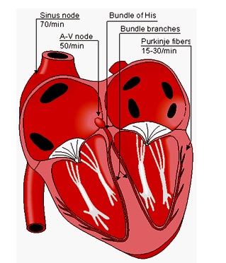
Figure 2.5. The conduction system of the heart.
Because the intrinsic rate of the sinus node is the greatest, it sets the activation frequency of the whole heart. If the connection from the atria to the AV node fails, the AV node adopts its intrinsic frequency. If the conduction system fails at the bundle of His, the ventricles will beat at the rate determined by their own region that has the highest intrinsic frequency. The electric events in the heart are summarized in Table 2.1. The waveforms of action impulse observed in different specialized cardiac tissue are shown in Figure 2.6.
Table 2.1. Electric events in the heart
| Location in the heart |
Event | Time [ms] | ECG- terminology |
Conduction velocity [m/s] |
Intrinsic frequency [1/min] |
||
| SA node atrium, Right Left AV nodebundle of His bundle branches Purkinje fibers endocardium Septum Left ventricle epicardium epicardium endocardium |
Impulse generated depolarization *) depolarization arrival of impulse departure of impulse activated activated activateddepolarization depolarization depolarization repolarization |
0 5 85 50 125 130 145 150175 190 225 400 600 |
P P P-Q intervalQRS T |
0.05 0.8-1.0 0.8-1.0 0.02-0.051.0-1.5 1.0-1.5 3.0-3.5 0.3 (axial) 0.5 |
70-80
20-40 |
||
| *) Atrial repolarization occurs during the ventricular depolarization; therefore, it is not normally seen in the electrocardiogram. |

Figure 2.6. Electrophysiology of the heart. The different waveforms for each of the specialized cells found in the heart are shown. The latency shown approximates that normally found in the healthy heart.
2.3. Theory of Operation of ECG
The electric potentials generated by the heart appear throughout the body and on its surface. We determine potential difference by placing electrodes on the surface of the body and measuring the voltage between them, being careful to draw little current (ideally there should be no current at all, because current distorts the electric field that produces the potential differences). If the two electrodes are located on different equal-potential lines of the electric field of the heart, a nonzero potential difference or voltage is measured. Different pairs of electrodes at different locations generally yield different voltages because of the spatial dependence of the electric field of the heart. Thus it is important to have certain standard positions of clinical evaluation of the ECG. The limbs make fine guideposts for locating the ECG electrodes. This is mentioned in more details in Appendix A.
In the simplified dipole model of the heart, it would be convenient if we could predict the voltage, or at least its waveform, in a particular set of electrodes at a particular instant of time when the cardiac vector is known. We can do this if we define a lead vector for the pair of electrodes. This vector is a unit vector that defines the direction a constant-magnitude cardiac vector must have to generate maximal voltage in the particular pair of electrodes. A pair of electrodes, or combination of several electrodes through a resistive network that gives an equivalent pair, is referred to as a lead.
In clinical electrocardiography, more than one lead must be recorded to describe the heart’s electric activity fully. In practice, several leads are taken in the frontal plane (the plane of the body that is parallel to the ground when one is lying on his back) and the transverse plane (the plane of the body that is parallel to the ground when one is standing erect).
The implementation we did was considering the limb leads, or they are scientifically called bipolar leads, hence they are described in much details while other types are shown in the Appendix.
2.3.1. Limb Leads
Augustus Désiré Waller measured the human electrocardiogram in 1887 using Lippmann’s capillary electrometer (Waller, 1887). He selected five electrode locations: the four extremities and the mouth (Waller, 1889). In this way, it became possible to achieve a sufficiently low contact impedance and thus to maximize the ECG signal. Furthermore, the electrode location is unmistakably defined and the attachment of electrodes facilitated at the limb positions. The five measurement points produce altogether 10 different leads (see Fig. 2.7A). From these 10 possibilities he selected five – designated cardinal leads. Two of these are identical to the Einthoven leads I and III described below.
Willem Einthoven also used the capillary electrometer in his first ECG recordings. His essential contribution to ECG-recording technology was the development and application of the string galvanometer. Its sensitivity greatly exceeded the previously used capillary electrometer. The string galvanometer itself was invented by Clément Ader (Ader, 1897). In 1908 Willem Einthoven published a description of the first clinically important ECG measuring system (Einthoven, 1908). The above-mentioned practical considerations rather than bioelectric ones determined the Einthoven lead system, which is an application of the 10 leads of Waller. The Einthoven lead system is illustrated in Figure 2.7B.

Figure 2.7. (A) The 10 ECG leads of Waller. (B) Einthoven limb leads and Einthoven triangle. The Einthoven triangle is an approximate description of the lead vectors associated with the limb leads. Lead I is shown as I in the above figure, etc.
The Einthoven limb leads (standard leads) are defined in the following way:
| Lead I: VI = ΦL – ΦR | |
| Lead II: VII = ΦF – ΦR | (2.1) |
| Lead III: VIII = ΦF – ΦL |
| where | VI | = the voltage of Lead I |
| VII | = the voltage of Lead II | |
| VIII | = the voltage of Lead III | |
| ΦL | = potential at the left arm | |
| ΦR | = potential at the right arm | |
| ΦF | = potential at the left foot |
(The left arm, right arm, and left leg (foot) are also represented with symbols LA, RA, and LL, respectively.)
According to Kirchhoff’s law these lead voltages have the following relationship:
| VI + VIII = VII | (2.2) |
hence only two of these three leads are independent.
The lead vectors associated with Einthoven’s lead system are conventionally found based on the assumption that the heart is located in an infinite, homogeneous volume conductor (or at the center of a homogeneous sphere representing the torso). One can show that if the position of the right arm, left arm, and left leg are at the vertices of an equilateral triangle, having the heart located at its center, then the lead vectors also form an equilateral triangle.
A simple model results from assuming that the cardiac sources are represented by a dipole located at the center of a sphere representing the torso, hence at the center of the equilateral triangle. With these assumptions, the voltages measured by the three limb leads are proportional to the projections of the electric heart vector on the sides of the lead vector triangle, as described in Figure 2.7B.
2.3.2. Formation of the ECG Signal
The cells that constitute the ventricular myocardium are coupled together by gap junctions which, for the normal healthy heart, have a very low resistance. As a consequence, activity in one cell is readily propagated to neighboring cells. It is said that the heart behaves as a syncytium; a propagating wave once initiated continues to propagate uniformly into the region that is still at rest.
It should be possible to examine the actual generation of the ECG by taking into account a realistic progression of activation double layers. Such a description is contained in Figure 2.8. After the electric activation of the heart has begun at the sinus node, it spreads along the atrial walls. The resultant vector of the atrial electric activity is illustrated with a thick arrow. The projections of this resultant vector on each of the three Einthoven limb leads is positive, and therefore, the measured signals are also positive.
After the depolarization has propagated over the atrial walls, it reaches the AV node. The propagation through the AV junction is very slow and involves negligible amount of tissue; it results in a delay in the progress of activation. (This is a desirable pause which allows completion of ventricular filling.)
Once activation has reached the ventricles, propagation proceeds along the Purkinje fibers to the inner walls of the ventricles. The ventricular depolarization starts first from the left side of the interventricular septum, and therefore, the resultant dipole from this septal activation points to the right. Figure 2.8 shows that this causes a negative signal in leads I and II.
In the next phase, depolarization waves occur on both sides of the septum, and their electric forces cancel. However, early apical activation is also occurring, so the resultant vector points to the apex.

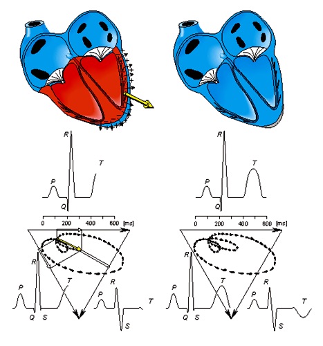
Figure 2.8. The generation of the ECG signal in the Einthoven limb leads.
After a while the depolarization front has propagated through the wall of the right ventricle; when it first arrives at the epicardial surface of the right-ventricular free wall, the event is called breakthrough. Because the left ventricular wall is thicker, activation of the left ventricular free wall continues even after depolarization of a large part of the right ventricle. Because there are no compensating electric forces on the right, the resultant vector reaches its maximum in this phase, and it points leftward. The depolarization front continues propagation along the left ventricular wall toward the back. Because its surface area now continuously decreases, the magnitude of the resultant vector also decreases until the whole ventricular muscle is depolarized. The last to depolarize are basal regions of both left and right ventricles. Because there is no longer a propagating activation front, there is no signal either.
Ventricular repolarization begins from the outer side of the ventricles and the repolarization front “propagates” inward. This seems paradoxical, but even though the epicardium is the last to depolarize, its action potential durations are relatively short, and it is the first to recover. Although recovery of one cell does not propagate to neighboring cells, one notices that recovery generally does move from the epicardium toward the endocardium. The inward spread of the repolarization front generates a signal with the same sign as the outward depolarization front. Because of the diffuse form of the repolarization, the amplitude of the signal is much smaller than that of the depolarization wave and it lasts longer.
The normal electrocardiogram is illustrated in Figure 2.9. The figure also includes definitions for various segments and intervals in the ECG. The deflections in this signal are denoted in alphabetic order starting with the letter P, which represents atrial depolarization. The ventricular depolarization causes the QRS complex, and repolarization is responsible for the T-wave. Atrial repolarization occurs during the QRS complex and produces such a low signal amplitude that it cannot be seen apart from the normal ECG.

Figure 2.9. The normal electrocardiogram.
2.3.3. The Information Content of The 12-Lead System
The most commonly used clinical ECG-system, which is the 12-lead ECG system, consists of the following 12 leads, which are:
| I, II, III | |
| aVR, aVL, aVF | |
| V1, V2, V3, V4, V5, V6 |
Of these 12 leads, the first six are derived from the same three measurement points. Therefore, any two of these six leads include exactly the same information as the other four.
Over 90% of the heart’s electric activity can be explained with a dipole source model. To evaluate this dipole, it is sufficient to measure its three independent components. In principle, two of the limb leads (I, II, III) could reflect the frontal plane components, whereas one precordial lead could be chosen for the anterior-posterior component. The combination should be sufficient to describe completely the electric heart vector. To the extent that the cardiac source can be described as a dipole, the 12-lead ECG system could be thought to have three independent leads and nine redundant leads.
However, in fact, the precordial leads detect also nondipolar components, which have diagnostic significance because they are located close to the frontal part of the heart. Therefore, the 12-lead ECG system has eight truly independent and four redundant leads. The lead vectors for each lead based on an idealized (spherical) volume conductor are shown in Figure 15.9. These figures are assumed to apply in clinical electrocardiography.
The main reason for recording all 12 leads is that it enhances pattern recognition. This combination of leads gives the clinician an opportunity to compare the projections of the resultant vectors in two orthogonal planes and at different angles. In summary, for the approximation of cardiac electric activity by a single fixed-location dipole, nine leads are redundant in the 12-lead system, as noted above.
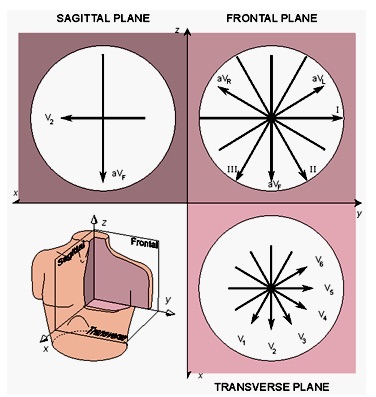
Figure 2.10. The projections of the lead vectors of the 12-lead ECG system in three orthogonal planes
2.4. The Basis of ECG Diagnosis
2.4.1. The Application Areas of ECG Diagnosis
The main applications of the ECG to cardiological diagnosis include the following (see also Figure 2.11):
- 1. The electric axis of the heart
- 2. Heart rate monitoring
- 3. Arrhythmias
- a. Supraventricular arrhythmias
- b. Ventricular arrhythmias
- 4. Disorders in the activation sequence
- . Atrioventricular conduction defects (blocks)
- a. Bundle-branch block
- b. Wolff-Parkinson-White syndrome
- 5. Increase in wall thickness or size of the atria and ventricles
- . Atrial enlargement (hypertrophy)
- a. Ventricular enlargement (hypertrophy)
- 6. Myocardial ischemia and infarction
- . Ischemia
- a. Infarction
- 7. Drug effect
- . Digitalis
- a. Quinidine
- 8. Electrolyte imbalance
Potassium
- . Calcium
- 9. Carditis
Pericarditis
Myocarditis
- 10. Pacemaker monitoring
Cardiac Rhythm Diagnosis and other heart disorders can be seen in full details in Appendix A

Figure 2.11 Application areas of ECG diagnosis.
2.4.2. Determination of The Electric Axis of The Heart
The concept of the electric axis of the heart usually denotes the average direction of the electric activity throughout ventricular (or sometimes atrial) activation. The term mean vector is frequently used instead of “electric axis.” The direction of the electric axis may also denote the instantaneous direction of the electric heart vector. The normal range of the electric axis lies between +30° and -110° in the frontal plane and between +30° and -30° in the transverse plane. (Note that the angles are given in the consistent coordinate system of the Appendix.)
The direction of the electric axis may be approximated from the 12-lead ECG by finding the lead in the frontal plane, where the QRS-complex has largest positive deflection. The direction of the electric axis is in the direction of this lead vector. The result can be checked by observing that the QRS-complex is symmetrically biphasic in the lead that is normal to the electric axis. The directions of the leads were summarized in Figure 2.10. Deviation of the electric axis to the right is an indication of increased electric activity in the right ventricle due to increased right ventricular mass. This is usually a consequence of chronic obstructive lung disease, pulmonary emboli, certain types of congenital heart disease, or other disorders causing severe pulmonary hypertension and corpulmonale.
Deviation of the electric axis to the left is an indication of increased electric activity in the left ventricle due to increased left ventricular mass. This is usually a consequence of hypertension, aortic stenosis, ischemic heart disease, or some intraventricular conduction defect.
The clinical meaning of the deviation of the heart’s electric axis is discussed in greater detail in connection with ventricular hypertrophy.
2.5. Electrocardiogram Electrodes
In order to measure and record potentials and, hence, currents in the body, it is necessary to provide some interface between the body and the electronic measuring apparatus. This interface function is carried out by biopotential electrodes. In any practical measurement of potentials, current flows in the measuring circuit for at least a fraction of the period of time over which the measurement is made. Ideally this current should be very small. However, in practical situations, it is never zero. Biopotential electrodes must therefore have the capability of conducting a current across the interface between the body and the electronic measuring circuit.
The electrode actually carries out a transducing function, because current is carried in the body by ions, whereas it is carried in the electrode and its lead wire by electrons. Thus the electrode must serve as a transducer to change an ionic current into an electronic current. This greatly complicates electrodes and places constraints on their operation. In appendix A there are much details about basic mechanisms involved in the transduction process and how they affect electrode characteristics rather than examining the principal electrical characteristics of biopotential electrodes (especially ECG). We shall here discuss electrical equivalent circuits for electrodes based on these characteristics. We shall then cover some of the different forms that ECG electrodes take in various types of ECG monitoring instrumentation systems.
2.5.1. Electrode Behavior and Circuit Models
The electrical characteristics of electrodes have been the subject of much study. Often the current-voltage characteristics of the electrode-electrolyte interface are found to be nonlinear, and, in turn, nonlinear elements are required for modeling electrode behavior. Specifically, the characteristics of an electrode are sensitive to the current passing through the electrode, and the electrode characteristics at relatively high current densities can be considerably different from those at low current densities. The characteristics of electrodes are also waveform-dependent. When sinusoidal currents are used to measure the electrode’s circuit behavior, the characteristics are also frequency dependent.
For sinusoidal inputs, the terminal characteristics of an electrode have both a resistive and a reactive component. Over all but the lowest frequencies, this situation can be modeled as a series resistance and capacitance. It is not surprising to see a capacitance entering into this model, because the Half-cell potential (see Appendix A) was the result of the distribution of ionic charge at the electrode-electrolyte interface that had been considered a double layer of charge. This, of course should behave as a capacitor—hence the capacitive reactance seen for real electrodes.
The series resistance-capacitance equivalent circuit breaks down at the lower frequencies, where this model would suggest an impedance going to infinity as the frequency approaches dc. To avoid this problem, it can be convert to a parallel RC circuit that has a purely resistive impedance at very low frequencies. If we combine this circuit with a voltage source representing the half-cell potential and a series resistance representing the interface effects and resistance of the electrolyte, we can arrive at the biopotential electrode equivalent circuit model shown in Figure 2.12.
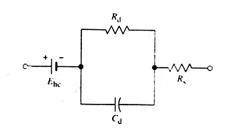
Figure 2.12. Equivalent circuit for a biopotential electrode in contact with an electrolyte
In this circuit, Rd and Cd represent the resistive and reactive components just discussed. These components are still frequency- and current-density-dependent. In this configuration it is also possible to assign physical meaning to the components. Cd represents the capacitance across the double layer of charge at the electrode-electrolyte interface. The parallel resistance Rd represents the leakage resistance across this double layer. All the components of this equivalent circuit have values determined by the electrode material, and ___to a lesser extent___ by the material of the electrolyte and its concentration.
The equivalent circuit of Figure 2.12 demonstrates that the electrode impedance is frequency-dependent. At high frequencies, where 1/ωC << Rd, the impedance is constant at Rs. At low frequencies, where 1/ωC >> Rd, the impedance is again constant but its value is larger, being Rs + Rd . At frequencies between these extremes, the electrode impedance is frequency-dependent.
2.5.2. The Electrode-Skin Interface and Motion Artifact
When biopotentials are recorded from the surface of the skin, we must consider an additional interface—the interface between the electrode-electrolyte and the skin—in order to understand the behavior of the electrodes. In coupling an electrode to the skin, we generally use a transparent electrolyte gel containing Cl– as the principal anion to maintain good contact. Alternatively, we may use an electrode cream, which contains Cl– and has the consistency of hand lotion. The interface between this gel and the electrode is an electrode-electrolyte interface. However, the interface between the electrolyte and the skin is different and requires some explanation. To represent the electric connection between an electrode and the skin through the agency of electrolyte gel, the equivalent circuit of Figure 2.12 must be expanded, as shown in Figure 2.13.
The electrode-electrolyte interface equivalent circuit is shown adjacent to the electrode-gel interface. The series resistance Rs is now the effective resistance associated with interface effects of the gel between the electrode and the skin. We can consider the epidermis of the skin as a membrane that is semipermeable to ions, so if there is a difference in ionic concentration across this membrane, there is a potential difference Ese, which is given by the Nernst equation. The epidermal layer is also found to have an electric impedance that behaves as a parallel RC circuit, as shown. For 1 cm2, skin impedance reduces from approximately 200 kΩ at 1 Hz to 200 Ω at 1 MHz. The dermis and the subcutaneous layer under it behave in general as pure resistances. They generate negligible dc potentials. Thus we see that a more stable electrode will result.
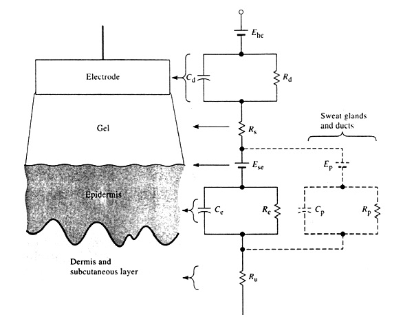
Figure 2.13. A body-surface electrode is placed against skin, showing the total electrical equivalent circuit.
There is a potential difference between the lumen of the sweat duct and the dermis and subcutaneous layers. There also is a parallel RpCp combination in series with this potential that represents the wall of the sweat gland and duct, as shown by the broken lines in Figure 2.13. When a polarizable electrode is in contact with an electrolyte, a double layer of charge forms at the interface. If the electrode is moved with respect to the electrolyte, this movement mechanically disturbs the distribution of charge at the interface and results in a momentary change of the half-cell potential until equilibrium can be reestablished. If a pair of electrodes is in an electrolyte and one moves while the other remains stationary, a potential difference appears between the two electrodes during this movement. This potential is known as motion artifact and can be a serious cause of interference in the measurement of biopotentials.
Because motion artifact results primarily from mechanical disturbances of the distribution of charge at the electrode-electrolyte interface, it is reasonable to expect that motion artifact is minimal for nonpolarizable electrodes (see the Appendix). Observation of the motion-artifact signals reveals that a major component of this noise is at low frequencies. The low-frequency artifact does affect signals such as ECG, EEG, and EOG. Consequently, it is important in these applications to use a nonpolarizable electrode to minimize motion artifact stemming from the electrode-electrolyte interface.
This interface, however, is not the only source of motion artifact encountered when biopotential electrodes are applied to the skin. The equivalent circuit in Figure 2.13 shows that, in addition to the half-cell potential Ehc the electrolyte gel-skin potential Ese can also cause motion artifact if it varies with movement of the electrode. Variations of this potential indeed do represent a major source of motion artifact in Ag/AgCl skin electrodes used in ECG. They have shown that this artifact can be significantly reduced when the most upper skin layer, named stratum corneum, is removed by mechanical abrasion with a fine abrasive paper. This method also helps to reduce the epidermal component of the skin impedance. Tarn and Webster (1977) also point out, however, that removal of the body’s outer protective barrier makes that region of skin more susceptible to irritation from the electrolyte gel. Therefore, the choice of a gel material is important. Remembering the dynamic nature of the epidermis, note also that the stratum corneum can regenerate itself in as short a time as 24 hours, thereby renewing the source of motion artifact. This is a factor to be taken into account if the electrodes are to be used for chronic recording as in monitoring . A potential between the inside and outside of the skin can be measured. Stretching the skin changes this skin potential by 5-10 mV, and this change appears as motion artifact. Ten 0.5-mm skin punctures through the barrier layer shortcircuits the skin potential and reduces the stretch artifact to less than 0.2 mV. De Talhouet and Webster (1996) provide a model for the origin of this skin potential and show how it can be reduced by stripping layers of the skin using Scotch tape.
2.5.3. Body-Surface Recording Electrodes for ECG
Over the years many different types of electrodes for recording various potentials on the body surface have been developed. This section describes only the types of these electrodes that are used in long durations so as to be appropriate with the monitoring application. The reader interested in more extensive examples should see Appendix A or consult Geddes (1972).
2.5.3.1.Metal-Plate Electrodes
It consists of a metallic conductor in contact with the skin. An electrolyte soaked pad or gel is used to establish and maintain the contact. Figure 2.14 shows several forms of this electrode. The one most commonly used for limb electrodes with the electrocardiograph is shown in Figure 2.14(a). It consists of a flat metal plate that has been bent into a cylindrical segment. A terminal is placed on its outside surface near one end; this terminal is used to attach the lead wire to the electrocardiograph. A post, placed on this same side near the center, is used to connect a rubber strap to the electrode and hold it in place on an arm or leg. Before it is attached to the body, its concave surface is covered with electrolyte gel. Similarly arranged flat metal disks are also used for this type of electrode, these traditional electrodes remain popular and are frequently used.
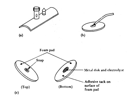
Figure 2.14. Body-surface biopotential electrodes
A second common variety of metal-plate electrode is the metal disk illustrated in Figure 2.14(b). This electrode, which has a lead wire soldered or welded to the back surface, can be made of several different materials. Sometimes the connection between lead wire and electrode is protected by a layer of insulating material, such as epoxy or polyvinyl chloride. This structure can be used as a chest electrode for recording the ECG or in cardiac monitoring for long-term recordings such as in ICUs. In these applications the electrode is often fabricated from a disk of Ag that may or may not have an electrolytically deposited layer of AgCl on its contacting surface. It is coated with electrolyte gel and then pressed against the patient’s chest wall. It is maintained in place by a strip of surgical tape or a plastic foam disk with a layer of tack on one surface.
Disk-shaped electrodes such as these have also been fabricated from metal foils (primarily silver foil) and are applied as single-use disposable electrodes. The thinness of the foil allows it to conform to the shape of the body surface. Also, because it is so thin, the cost can be kept relatively low.
Economics necessarily plays an important role in determining what materials and apparatus are used in hospital administration and patient care. In choosing suitable cardiac electrodes for patient-monitoring applications, physicians are more and more turning to pregelled, disposable electrodes with the adhesive already in place. These devices are ready to be applied to the patient and are not cleaned after use. This minimizes the amount of time that personnel must devote to the use of these electrodes.
A popular type of electrode of this variety is illustrated in Figure 2.14(c). It consists of a relatively large disk of plastic foam material with a silver-plated disk on one side attached to a silver-plated snap similar to that used on clothing in the center of the other side. A lead wire with the female portion of the snap is then snapped onto the electrode and used to connect the assembly to the monitoring apparatus. The silver-plated disk serves as the electrode and may be coated with an AgCl layer. A layer of electrolyte gel covers the disk. The electrode side of the foam is covered with an adhesive material that is compatible with the skin. A protective cover or strip of release paper is placed over this side of the electrode and foam, and the complete electrode is packaged in a foil envelope so that the water component of the gel will not evaporate away. To apply the electrode to the patient, the technician has only to clean the area of skin on which the electrode is to be placed, open the electrode packet, remove the release paper from the tack, and press the electrode against the patient. This procedure is quickly accomplished and no special technique need be learned, such as using the correct amount of gel or cutting strips of adhesive tape to hold the electrode in place. This type of electrodes is the used one in our implementation. We have already fabricated one using simple material as will be described later in the text.
2.5.3.2. Suction Electrodes
On the other hand there is a modification of the metal-plate electrode that requires no straps or adhesives for holding it in place is the suction electrode illustrated in Figure 2.15. Such electrodes are frequently used in electrocardiography as the precordial (chest) leads, because they can be placed at particular locations and used to take a recording. They consist of a hollow metallic cylindrical electrode that makes contact with the skin at its base. An appropriate terminal for the lead wire is attached to the metal cylinder, and a rubber suction bulb fits over its other base. Electrolyte gel is placed over the contacting surface of the electrode, the bulb is squeezed, and the electrode is then placed on the chest wall. The bulb is released and applies suction against the skin, holding the electrode assembly in place. This electrode can be used only for short periods of time; the suction and the pressure of the contact surface against the skin can cause irritation. Although the electrode itself is quite large, Figure 2.15 shows that the actual contacting area is relatively small.
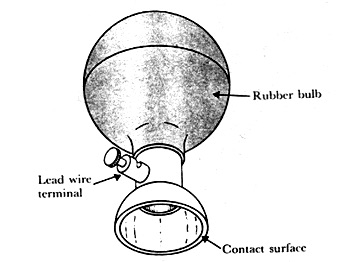
Figure 2.15. A metallic suction electrode
This electrode thus tends to have a higher source impedance than the relatively large-surface-area metal-plate electrodes used for ECG limb electrodes, as shown in Figure 2.14(a). Generally, the electrodes have standards to be implemented. In the Appendix are some of them in addition to some practical hints when using them.
2.6. Functional Blocks of The Electrocardiograph
Figure 2.16 shows a block diagram of a typical clinical electrocardiograph as a standardization.
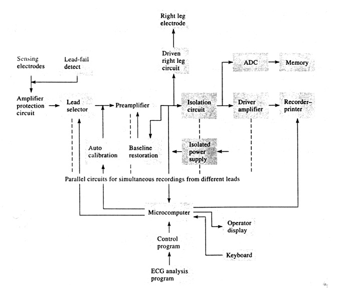
Figure 2.16. Block diagram of an electrocardiograph
To understand the overall operation of the system, let us consider each block separately.
1. Protection circuit This circuit includes protection devices so that the high voltages that may appear across the input to the electrocardiograph under certain conditions do not damage it.
2. Lead selector Each electrode connected to the patient is attached to the lead selector of the electrocardiograph. The function of this block is to determine which electrodes are necessary for a particular lead and to connect them to the remainder of the circuit. It is this part of the electrocardiograph in which the connections for the central terminal are made. This block can be controlled by the operator or by the microcomputer of the electrocardiograph when it is operated in automatic mode. It selects one or more leads to be recorded.
3. Calibration Signal A 1-mV calibration signal is momentarily introduced into the electrocardiograph for each channel that is recorded.
4. Preamplifier The input preamplifier stage carries out the initial amplification of the ECG. This stage should have very high input impedance and a high common-mode-rejection ratio (CMRR). A typical preamplifier stage is the differential amplifier that consists of three operational amplifiers, shown in Figure 2.17. A gain-control switch is often included as a part of this stage.
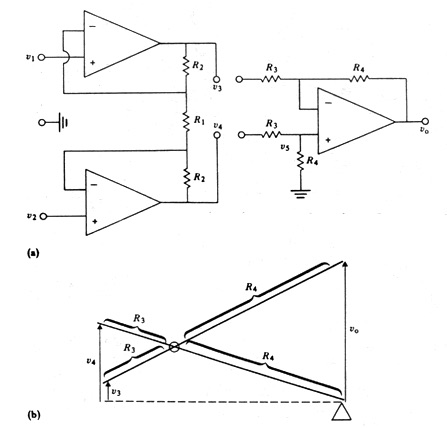
Figure 2.17. An Instrumentation Amplifier
5. Isolation circuit The circuitry of this block contains a barrier to the passage of current from the power line (50 or 60 Hz). For example, if the patient came in contact with a 120-V line, this barrier would prevent dangerous currents from flowing from the patient through the amplifier to the ground of the recorder or microcomputer.
6. Driven right leg circuit This circuit provides a reference point on the patient that normally is at ground potential. This connection is made to an electrode on the patient’s right leg. Details on this circuit are given later on.
7. Driver amplifier Circuitry in this block amplifies the ECG to a level at which it can appropriately record the signal on the recorder. Its input should be ac-coupled so that offset voltages amplified by the preamplifier are not seen at its input. These dc voltages, when amplified by this stage, might cause it to saturate. This stage also carries out the bandpass filtering of the Electrocardiograph to give the frequency characteristics described in Table 2.2 below. Also it often has a zero-offset control that is used to position the signal on the chart paper. This control adjusts the dc level of the output signal
8. memory system Many modern electrocardiographs store electrocardiograms in memory as well as printing them out on a paper chart. The signal is first digitized by an ADC, and then samples from each lead are stored in memory. Patient information entered via the keyboard is also stored. The microcomputer controls this storage activity.
9. Microcomputer The microcomputer controls the overall operation of the electrocardiograph. A keyboard and a display enable the operator to communicate with the microcomputer.
10. Recorder-printer This block provides a hardcopy of the recorded ECG signal. It also prints out patient identification, clinical information entered by the operator, and the results of the automatic analysis of the electrocardiogram.
Specific Requirements of The Electrocardiograph
Because the electrocardiograph is widely used as a diagnostic tool and there are several manufacturers of this instrument, standardization is necessary. Standard requirements for electrocardiographs have been developed over the years (Bailey et al. 1990; Anonymous, 1991).
Table 2.2 gives a summary of performance requirements from the most recent of these (Anonymous, 1991). These recommendations are a part of a voluntary standard. The Food and Drug Administration is planning to develop mandatory standards for frequently employed instruments such as the electrocardiograph.
Table 2.2 Summary of Performance Requirements for Electrocardiographs (Anonymous, 1991)
| Requirement Description | Min/max | Units | Min/max value |
| Operating Conditions: | |||
| line voltage | range | V rms | 104 to 1127 |
| Frequency | range | Hz | 50 or 60 ± 1 |
| Temperature | range | °C | 25 ± 10 |
| relative humidity | range | % | 50 ± 20 |
| atmospheric pressure | range | Pa | 7 X 10⁴ to
10.6 X 10⁴ |
| Input Dynamic Range: | |||
| range of linear operations of input signal | min | mV | ±5 |
| slew rate change | max | mV/s | 320 |
| dc offset voltage range | min | mV | ±300 |
| Allowed variation of amplitude with dc offset | max | % | ±5 |
| Gain Control, Accuracy, and Stability: | |||
| gain selections | min | mm/mV | 20, 10, 5 |
| gain error | max | % | 5 |
| gain change rate/minute | max | % /min | ±0.33 |
| total gain change/hour | max | % | ±3 |
| Time Base Selection and Accuracy: | |||
| Time base selections | min | mm/s | 25, 50 |
| time base error | max | % | ±5 |
| Output Display: | |||
| width of display | min | mm | 40 |
| trace visibility (writing rates) | max | mm/s | 1600 |
| trace width (permanent record only) | max | mm | 1 |
| departure from time | max | mm | 0.5 |
| axis alignment | max | ms | 10 |
| preruled paper division | min | div/cm | 10 |
| error of rulings | max | % | ±2 |
| time marker error | max | % | ±2 |
| Accuracy of Input Signal Reproduction: | |||
| overall error for signals | max | % | ±5 |
| up to ± 5 mV and 125 mV/s | max | µV | ±40 |
| upper cut-off frequency (3 dB) | min | Hz | 150 |
| response to 20 ms, 1.5 mV triangular input | min | mm | 13.5 |
| response after 3 mV, 100 ms impulse | max | mV | 0.1 |
| max | mV/s | 0.30 | |
| error in lead weighting factors | max | % | 5 |
| Standardizing Voltage: | |||
| nominal value | NA | mV | 1.0 |
| rise time | max | ms | 1 |
| decay time | min | s | 100 |
| amplitude error | max | % | ±5 |
| Input Impedance at 10 Hz (each lead) | min | MΩ | 2.5 |
| DC Current (any input lead) | max | µA | 0.1 |
| DC Current (any patient electrode) | max | µA | 1.0 |
| Common-Mode Rejection: | |||
| Allowable noise with 20 V, 60 Hz and ± 300 mV dc and 51 kΩ |
max |
mm | 10 |
| System Noise: | |||
| RTI, p-p | max | µV | 30 |
| multichannel crosstalk | max | % | 2 |
| Baseline Control and Stability: | |||
| return time after reset | max | s | 3 |
| return time after lead switch | max | s | 1 |
| Baseline Stability: | |||
| baseline drift rate RTI | max | µV/s | 10 |
| total baseline drift RTI (2-min period) | max | µV | 500 |
| Overload Protection: | |||
| no damage from differential voltage, | |||
| 60-Hz, 1-V p-p, 10-s application | min | V | 1 |
| no damage from simulated defibrillator | |||
| discharges: | |||
| overvoltage | N/A | V | 5000 |
| energy | N/A | J | 360 |
| recovery time | max | s | 8 |
| energy reduction by defibrillator | |||
| shunting | max | % | 10 |
| transfer of charge through defibrillator
chassis |
max | µC | 100 |
| ECG display in presence of pacemaker
pulses: |
|||
| amplitude | range | mV | 2 to 250 |
| pulse duration | range | ms | 0.1 to 2.0 |
| rise time | max | µs | 100 |
| frequency | max | pulses/min | 100 |
| Risk Current (Isolated Patient Connection) | Max | µA | 10 |
| Auxiliary Output (if provided): | |||
| no damage from short circuit risk current (isolated patient connection) | max | µA | 10 |
2.7. Distortion Factors in The ECG
It was pointed out that uncorrected lead systems evince a considerable amount of distortion affecting the quality of the ECG signal. In the corrected lead systems many of these factors are compensated for by various design methods. Distortion factors arise, generally, because the preconditions are not satisfied.
None of these assumptions are met clinically, and therefore, the ECG signal deviates from the ideal. In addition, there are errors due to incorrect placement of the electrodes, poor electrode-skin contact, other sources of noise, and finally instrumentation error. The character and magnitude of these inaccuracies are discussed in great details in Appendix A. Only some of them, which are with respect to the apparatus itself, are summarized here.
2.7.1. Frequency Distortion
The electrocardiograph does not always meet the frequency-response standards we have described. When this happens, frequency distortion is seen in the ECG.
High-frequency distortion rounds off the sharp corners of the waveforms and diminishes the amplitude of the QRS complex.
2.7.2. Saturation Or Cutoff Distortion
High offset voltages at the electrodes or improperly adjusted amplifiers in the electrocadiograph can produce saturation or cutoff distotion that can greatly modify the appearance of the ECG. The combination of input-signal amplitude and offset voltages drives the amplifier into saturation during a portion of the QRS complex. the peaks of the QRS complex are cut off because the output of the amplifier cannot exceed the saturation voltage.
In a similar occurrence, the lower portion of the ECG are cut off. This can result from negative saturation of the amplifier. In this case only a portion of the S-wave may be cut off. In extreme cases of this type of distortion even the P and T waves may be below the cutoff level such that only the R wave appears.
2.7.3. Ground Loops
Patients who are having their ECGs taken on either a clinical electrocardiograph or continuously on a cardiac monitor are often connected to other pieces of electric apparatus. Each electric device has its own ground connection either through the power line or, in some cases, through a heavy ground wire attached to some ground point in the room.
A ground loop can exist when two machines are connected to the patient. Both the electrocardiograph and a second machine have a ground electrode attached to the patient. The electrocardiograph is grounded through the power line at a particular socket. The second machine is also grounded through the power line, but it is plugged into an entirely different outlet across the room, which has a different ground. If one ground is at a slightly higher potential than the other ground, a current from one ground flows through the patient to the ground electrode of the electrocardiograph and along its lead wire to the other ground. In addition to this current’s presenting a safety problem, it can elevate the patient’s body potential to some voltage above the lowest ground to which the instrumentation is attached. This produces common-mode voltages on the electrocardiograph that, if it has a poor common-mode-rejection ratio, can increase the amount of interference seen.
2.7.4. Open Lead Wires
Frequently one of the wires connecting a biopotential electrode to the electrocardiograph becomes disconnected from its electrode or breaks as a result of excessively rough handling, in which case the electrode is no longer connected to the electrocardiograph. Relatively high potentials can often be induced in the open wire as a result of electric fields emanating from the power lines or other sources in the vicinity of the machine. This causes a wide, constant-amplitude deflection of the pen on the recorder at the power-line frequency, as well as, of course, signal loss. Such a situation also arises when an electrode is not making good contact with the patient. For such an error a circuit for detecting poor electrode contact is almost implemented
2.7.5. Artifact from Large Electric Transient
In some situations in which a patient is having an ECG taken, cardiac defibrillation may be required. In such a case, a high-voltage high-current electric pulse is applied to the chest of the patient so that transient potentials can be observed across the electrodes. These potentials can be several orders of magnitude higher than the normal potentials encountered in the ECG. Other electric sources can cause similar transients. When this situation occurs, it can cause an abrupt deflection in the ECG, as shown in Figure 2.18. This is due to the saturation of the amplifiers in the electrocardiograph caused by the relatively high-amplitude pulse or step at its input. This pulse is sufficiently large to cause the buildup of charge on coupling capacitances in the amplifier, resulting in its remaining saturated for a finite period of time following the pulse and then slowly drifting back to the original baseline with a time constant determined by the low corner frequency of the amplifier. The slowly recovering waveform is shown in Figure 2.18.
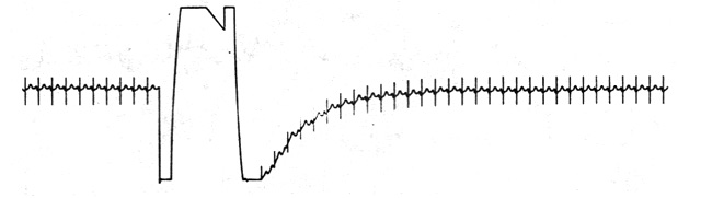
Figure 2.18. Effect of a voltage transient on an ECG.
Transients of the type just described can be generated by means other than defibrillation. Serious artifact caused by motion of the electrodes can produce variations in potential greater than ECG potentials. Another source of artifact is the patient’s encountering a built-up static electric charge that can be partially discharged through the body.
This problem is greatly alleviated by reducing the source of the artifact. Because we do not have time to disconnect an electrocardiograph when a patient is being defibrillated, we can include electronic protection circuitry in the machine itself. In this way, we can limit the maximal input voltage across the ECG amplifier so as to minimize the saturation and charge buildup effects due to the high-voltage input signals. This results in a more rapid return to normal operation following the transient. Such circuitry is also important in protecting the electrocardiograph from any damage that might be caused by these pulses.
Artifact caused by static electric charge on personnel can be lessened noticeably by reducing the buildup of static charge through the use of conductive clothing, shoes, and flooring, as well as by having personnel touch the bed before touching the patient.
2.7.6. Interference from Electric Devices
A major source of interference when one is recording or monitoring the ECG is the electric-power system. Besides providing power to the electrocardiograph itself, power lines are connected to other pieces of equipment and appliances in the typical hospital room or physician’s office. There are also power lines in the walls, floor, and ceiling running past the room to other points in the building. These power lines can affect the recording of the ECG and introduce interference at the line frequency in the recorded trace, as illustrated in Figure 2.19(a). Such interference appears on the recordings as a result of two mechanisms, each operating singly or, in some cases, both operating together.
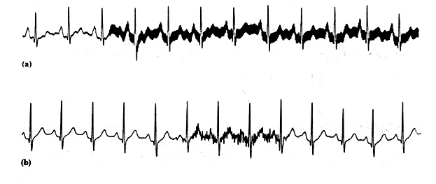
Figure 2.19. (a) 50-Hz power-line interference. (b) EMG interference on the ECG.
Electric-field coupling between the power lines and the electrocardiograph and/or the patient is a result of the electric fields surrounding main power lines and the power cords connecting different pieces of apparatus to electric outlets. These fields can be present even when the apparatus is not turned on, because current is not necessary to establish the electric field. These fields couple into the patient, the lead wires, and the electrocardiograph itself.
The other source of interference from power lines is magnetic induction. Current in power lines establishes a magnetic field in the vicinity of the line. Magnetic fields can also sometimes originate from transformers and ballasts in fluorescent lights.
2.7.7. Interference Reduction Circuit
Bioelectric recordings are often disturbed by an excessive level of interference. Although its origin in nearly all cases is clear -the main power supply – the cause of the disturbance is not at all obvious because in many cases very sophisticated equipment is used. Apparently, the use of equipment with very good specifications does not guarantee interference free recordings. In this paper it is argued that if a significant reduction of the level of intrference is persued, the whole measurement situation has to be analised.
In most bioelectric measurements an interference level of 1 – 10 microV,p-p (less than 1% of the peak-peak value of an ECG) is acceptable. As the noise of a typical electrode is also several microV,p-p (Geddes and Baker, 1966a; Spekhorst et al., 1988), in most circumstances 10 microV,p-p can be accepted as the upper level of interference. The most common mechanisms of electrical mains interference are described in the Appendix. In this section we concentrate greatly on the use of right leg driven circuit mentioned in the functional block diagram in the 5th section.
Driven-Right-Leg System
In many modern electrocardiographic systems, the patient is not grounded at all. Instead, the right-leg electrode is connected (as shown in Figure 2.20 to the output of an auxiliary op amp. The common-mode voltage on the body is sensed by the two averaging resistors Ra, inverted, amplified, and fed back to the right leg. This negative feedback drives the common-mode voltage to a low value. The body’s displacement current flows not to ground but rather to the op-amp output circuit. This reduces the pickup as far as the ECG amplifier is concerned and effectively grounds the patient.
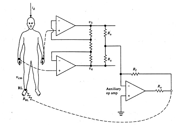
Figure 2.20. Driven-right-leg circuit for minimizing common-mode interference
The circuit can also provide some electric safety. If an abnormally high voltage should appear between the patient and ground as a result of electric leakage or other cause, the auxiliary op amp in Figure 2.20 saturates. This effectively ungrounds the patient, because the amplifier can no longer drive the right leg. Now the parallel resistances Rf and Ro are between the patient and ground. They can be several megohms in value—large enough to limit the current. These resistances do not protect the patient, however, because 120 V on the patient would break down the op-amp transistors of the ECG amplifier, and large currents would flow to ground.
2.7.8. Other Sources of Electric Interference
Electric interference from sources other than the power lines can also affect the electrocardiograph. Electromagnetic interference from nearby high-power radio, television, or radar facilities can be picked up and rectified by the p-n junctions of the transistors in the electrocardiograph and sometimes even by the electrode-electrolyte interface on the patient. The lead wires and the patient serve as an antenna. Once the signal is detected, the demodulated signal appears as interference on the electrocardiogram.
Electromagnetic interference can also be generated by high-frequency generators in the hospital itself. Electrosurgical and diathermy equipment is a frequent offender. Grobstein and Gatzke (1977) show both the proper use of electrosurgical equipment and the design of an ECG amplifier required to minimize interference. Electromagnetic radiation can be generated from x-ray machines or switches and relays on heavy-duty electric equipment in the hospital as well. Even arcing in a fluorescent light that is flickering and in need of replacement can produce serious interference.
There is also a source of electric interference located within the body itself that can have an effect on ECGs. There is always muscle located between the electrodes making up a lead of the electrocardiograph. Any time this muscle is contracting, it generates its own electromyographic signal that can be picked up by the lead along with the ECG and can result in interference on the ECG, as shown in Figure 2.19(b). When we look only at the ECG and not at the patient, it is sometimes difficult to determine whether interference of this type is muscle interference or the result of electromagnetic radiation. However, while the ECG is being taken, we can easily separate the two sources, because the EMG interference is associated with the patient’s muscle contractions.
2.8. Analog System Design and Criteria (Materials and Methods)
In this section the implementation of the project will be described in details. The first section reveals the general block diagram of the system. For each block a brief discussion is added. Besides, the circuit diagram corresponding to the block is also described briefly. Any details about the components characteristics may be found in Appendix C.
2.8.1 General block diagram.
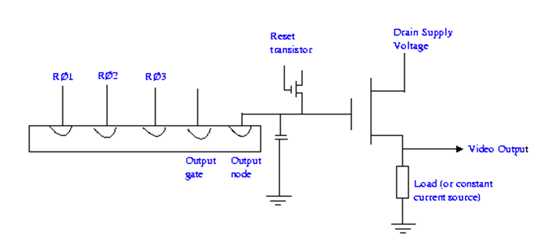
Figure . shows a simplified block diagram of the Electrocardiograph implementation of the ICU monitor project. It consists mainly the sensing electrodes, an instrumentation amplifier with high CMRR to pick up the weak signal and reject the noise. The further step is the filtration of signal to be in the range from 0.5 to 45 Hz as stated in the standard of patient monitors. An ADC is used to digitize the signal to be processed by a high speed Microcontroller unit. This unit also selects the lead vector to be displayed and also controls the gain of the ECG signal. The controlling and additional information is entered by a Keypad and the signal is displayed by an LCD.
The details of the Analog Blocks and Circuits are described in the next section. The digital part and signal acquisition are explained in full details in chapter 5, in which the hole digital system of the monitor is fully described.
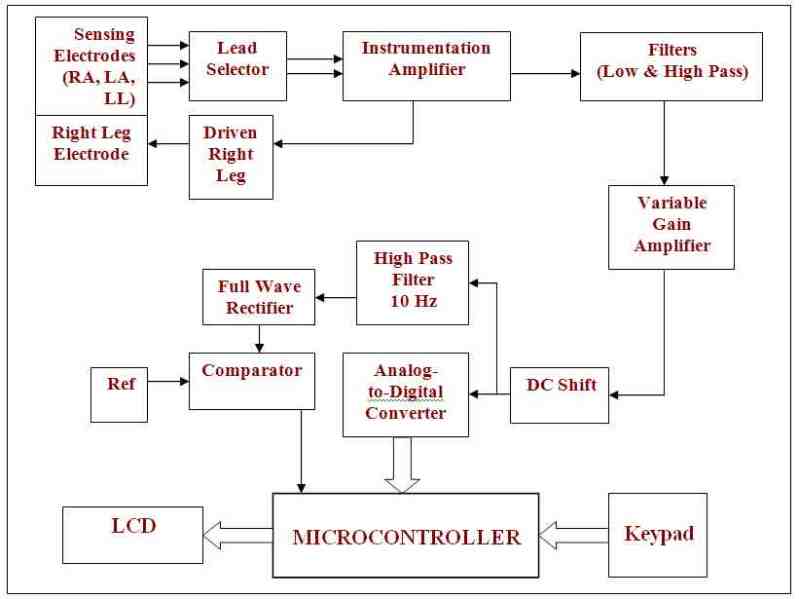
Figure 2.21 : Block Diagram of The Electrocardiograph
2.8.2. Details of Each Block:
1. Sensing Electrodes:
They are used to measure the electric potential between leads using the approach of bipolar lead vector described in previous sections. The front end of an ECG sensor must be able to deal with the extremely weak nature of the signal it is measuring. Even the strongest ECG signal has a magnitude of less than 10mV, and furthermore the ECG signals have very low drive (very high output impedance).
Electrodes are used for sensing bioelectric potentials as caused by muscle and nerve cells. ECG electrodes are generally of the direct-contact type. They work as transducers converting ionic flow from the body through an electrolyte into electron current and consequently an electric potential able to be measured by the front end of the ECG system. The figure below shows the two types of the electrodes used in the monitor project.
Lead wire cable:
We made a lead wire cable by using a shielded coaxial cable and snap similar to that use in clothing, the shielding around the central cable connected to the ground and the central cable connected to snap.
2. Leads selector:
The function of this stage is to determine which electrodes are necessary for a particular lead and hence selecting them. The leads of choice are leads I, П and Ш. The dual analog multiplexer (CD4052) is used to perform this task. It is shown below with its controlling parameters.
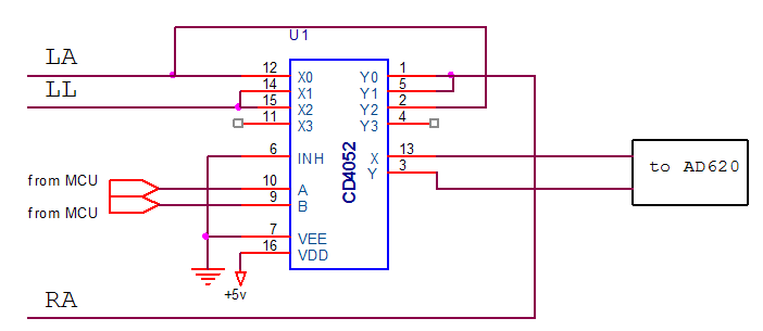
Figure 2.22. lead selector
The dual analog multiplexer (CD4052BC) is digitally controlled analog switches having low on impedance and very low off leakage currents. Control of analog signals up to 15Vp-p can be achieved by digital signal amplitudes of 3.16V. When a logical 1 is present at the inhibit input terminal all channels are off.
This type (CD4052BC) is a differential 4-channel multiplexer having two binary control inputs, A and B. The two binary input signals select 1 of 4 pairs of channels to be turned on and connect those differential analog inputs to the differential outputs.
3. Instrumentation Amplifier (IA) or Preamplifier:
The purpose of this stage is to reject noise and amplify the signal from the sensor electrodes, which typically falls in the 1 mV range, by a factor of 10. The basic architecture of this step follows a standard ECG monitoring circuit, found in most medical instrumentation textbooks. It functions by measuring the voltage difference between the two connected leads.
The instrumentation amplifier acts as the front-end for a signal acquisition system. The AD620 is chosen as it is a high precision amplifier commonly used in bio-electronics, featuring a measured CMRR of at least 100dB, a low cost, a max supply current of 1.3 mA and a wide power supply range (2.3V to 18V & -2.3V to –18V). It is also easy to use rather than its higher performance than three Operational Amplifiers IA design. The low power and signal accuracy are also important factors when choosing such an amplifier. This is due to its very low input bias current (10 nA) and offset voltage (50 µV), respectively. The figure below shows the AD620 as it is connected in our circuit.
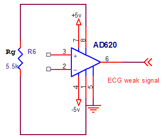
Figure 2.23. Instrumentation amplifier
Gain is set by a single external resistor to be in the range of 1 to 1000 and is given by the equation:
G = 1 + 49.4 kΩ / RG
An RG=5.5 kΩ is selected so that to obtain a gain of 10.
4. Driven Right leg:
This stage provides a reference point on the patient that normally is at ground potential. It is implemented in ECG measurement systems to counter common mode noise in the body. This circuit is as shown in Figure 2.24. The two signals entering the differential amplifier are summed then inverted and amplified in the right leg driver before being feed-backed to an electrode attached to the right leg. The other electrodes also pick up this signal and hence the noise is cancelled.
Without the driven right leg circuit a direct ground path is provided, which hence introduce risk of a ground fault hazard. With the right leg driven circuit provided, the body’s displacement current flows not to ground but rather to the Op Amp output circuit as shown below.
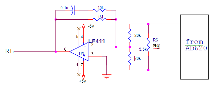
Figure 2.24. Driven Right leg circuit
We use the LF 411 for diversity of reasons including low cost, high speed, very low input offset voltage (which causes high signal accuracy), it requires low supply current yet maintain a large gain band width product.
5. Signal Filtering.
This block removes the undesirable noise. The two approaches for such a purpose are done through either the use of analogue circuitry or digital signal processing. The weak nature of the ECG signal and the great noise affecting it require multiple stages of filters to be implemented. Topologies and properties of the used filters are described in details here. We use three types of filters low pass, high pass and notch filters.
a- Low Pass Filter:
As a standardization of ECG monitors the frequency range of the displayed signal is to be from 0.5 to 45Hz. The low pass filter can remove a large amount of ambient noise and is responsible of ensuring these do not affect the ECG obtained.
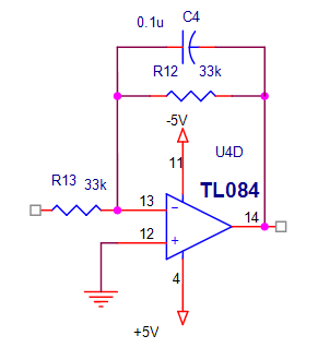
Figure 2.25. Active low pass filter
The low pass filter implemented is shown in Figure 2.25. It is a first order active filter. The corner frequency is calculated to be 45Hz. from the equation f =1\2πRC, substituting the value of C=0.1µf then the value of R=33KΏ. In the filter implementation the operational amplifier TL084 is used for many reasons low cost, low power consumption, low input bias and offset current, high input impedance. And the response of the low pass filter is shown in the figure below:
b- High pass Filter:
The high pass filter implemented is shown in the Figure below. We use passive high pass filter. The corner frequency is calculated at 0.5 Hz from the equation f =1\2πRC. Substituting the value of C=22 µf, then the value of R=14.75 kΏ.
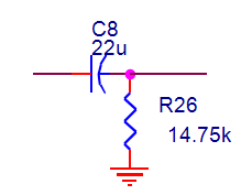
Figure 2.26. passive high pass filter at 0.5 HZ
Passive filters make no use of amplifying circuitry such as transistors or op-amps and as such are not constrained by the bandwidth limitation of these devices. The other major advantages are the fact that they require no power supply and the fact that they generate less noise.
Also we use a high pass filter (active high pass filter) at frequency corner 10 Hz to calculate heart rate, The frequency corner calculated by equation f =1\2πRC, substitute the value of C=1µf then the value of R=15 kΏ. We use also the operational amplifier TL084. The active high pass filter implemented is shown in the figure below:
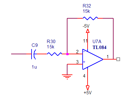
Figure 2.27. Active high pass filter at 10 Hz
6. Amplification Stage and Variable Gain Amplifier.
The purpose of this stage is to amplify the ECG signal coming from the filtering stage. We use TL084 operational amplifier to produce gain of 50. The amplification implemented is shown in figure below:
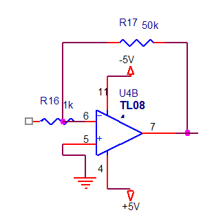
Figure 2.28. Gain Amplifier
We implement then a variable gain amplifier to produce different gains 2, 4, 8 and 10 by using op amp TL084 and accompanied by an analog multiplexer (CD 4051). The variable gain amplifier implemented is shown in Figure below:
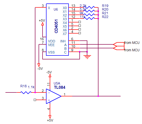
Figure 2.29. Variable Gain Amplifier
7. DC Shift.
After filtering and amplification, the data is ready to be digitized by the ADC0808. The ADC0808 requires the signal it is sampling to be completely in the positive voltage range. The summing amplifier is used to achieve this and its topology is shown in Figure.
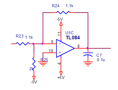
Figure 2.30. DC shift circuit
8. Full Wave Rectifier Circuit.
We use this circuit after the high pass filter (10Hz) for rectifying the signal then we introduce the output of this circuit to a comparator for calculating the heart rate, this comparator used for passing peaks of the ECG signal to obtain number of heart beats by further calculation at the microcontroller unit. The full wave rectifier circuit implemented is shown in Figure below:
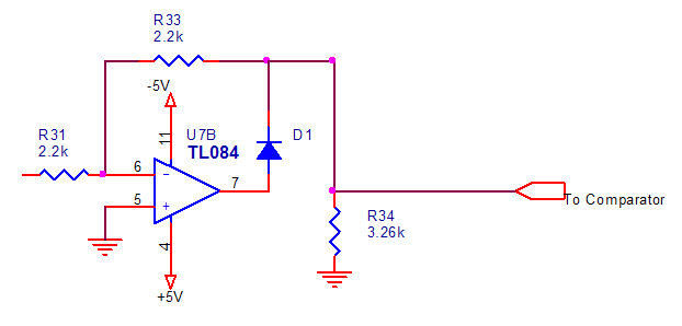
Figure 2.31. Full wave rectifier circuit
9. The Analog-To-Digital Converter
This stage is considered the most important stage in our system because it converts the signal from the analog form to the digital form so that further calculations and processing are maintained in the microcontroller. The accurate selection of sampling rate is very important.
In our design we use ADC0808 because of its sufficient conversion time for the application, accuracy and low cost. It has the following specs:
- • Resolution 8 Bits
- • Total Unadjusted Error ±1.2 LSB and ±1 LSB
- • Single Supply 5 VDC
- • Low Power 15 mW
- • Conversion Time 100 µs
In our application we consider the maximum frequency in the signal to be like the corner frequency of the low pass filter and more over we sampled one channel so the sampling rate must be more than 2 *fm (maximum frequency component) Hz, according to Nyquest theorem. As to be more practical we have sampled the signal by (8 * fm) which is controlled by the microcontroller. The input clock of the ADC0808 is 640 kHz as its datasheet suggests. This clock is supplied from the trigger circuit. The output digital data is then fed to the microcontroller through an octal buffer to protect our circuit from overloading when it is connected to the microcontroller to be more safer and practical.

Figure 2.32. Analog To Digital Converter
2.9. Results and Conclusion (Problems while implementing the hardware)
May be the lack of experience was the first problem to face us. One should first get very well in the topic via a very good background about it. Some disciplines should be well-learned first, such as physiology, microprocessors, digital and analog circuits and systems…, etc.
The first step therefore, which is the base of the project’s pyramid, was a very wide knowledge base. To be more efficient, a chapter about design criteria was added in this text so as to reveal how the engineers, especially the biomedical, should think about a design and offering good implementation of the problem.
The second problem was how to make our design as simple as possible then try to practice it as to be more professional. The next problem was the great lack of materials, especially the electronics material in the market.
In the ECG analog implementation we have designed the circuit without any patient safety consideration in a bred board, constructing first the instrumentation amplifier without the driven right leg circuit, and even without any filtrations.
As we have moderate results we start implementing some signal filtrations and amplifications. Actually the analog filtration was very complicated due to the very high noise and unsharpness that we noticed in the signal. To solve these problems, we put three low pass filters of nearly the same cut off frequency, hence as a total it was a third order low pass. In the high pass stage we have tried both the active and passive types but the passive one revealed better signal. Following this was the amplification circuit, then we make a variable gain amplifier to produce many gain selections. Afterwards the lead selector was constructed to select any required lead from three bipolar leads I, П and Ш.
As a pre-final step in the analog part the driven right leg circuit is implemented and we have made a lead wire cable due to the great noise we were encountering.
As an ensurence step before implementing the digital part we take the analog signal and display it on the digital oscilloscope, and take this signal by analog to digital converter (ADC0808) and to be displayed on the PC via parallel port by a small program.
The figure below show the signal of ECG taken from a simulator and displayed on a digital oscilloscope before start working on the digital part of the monitor.
The enclosed CD-ROM includes a gallery of the signal step by step on the digital oscilloscope. The final result of the analog part can be seen in figure 2.33.

Figure 2.33. The Analog Circuit (The signal displayed on the digital oscilloscope)