
This was a report I wrote in 2001 and I though it is good to share as is. Please excuse my poor language at that time and that I missed writing the references. Still I hope you will find good information about the topic if you are interested.
Abstract
One reason I got motivated to write about CCD is its existence in a variety of medical and non-medical equipment especially whenever we have digital imaging systems including x-ray, endoscopes cameras, extra- and intra-oral cameras…etc. One important point to say is using such a sensor could be a very active way to avoid many of the dangerous factors of such systems e.g. it can lessen the dose required for an x-ray image to about 80% of the dose when using an x-ray film.
In this report I will have some explanations about
1. What is a CCD?
2. Some basics of CCD.
3. Theory and Operation of CCD.
4. How CCD record color or distinguish among photons of different energies.
5. Some aspects of CCD behavior (characteristics)
6. Different types of CCDs.
7. Noise sources in CCD.
8. Some methods to test the performance of CCD camera.
9. Why CCD is so great. (Advantages and Early limitations)
10. Some biomedical applications of CCD.
11. Future of CCD.
1.What is a Charged-Coupled Device?
1.1.Overview on Photographic Detectors
Photographic plates were ubiquitous. The advantages that they offered were basically threefold:
- • Unlike the eye they were an integrating detector: fainter objects could be detected by making longer exposures to accumulate more light,
- • The images were objective and reproducible (unlike a sketch)
- • The photographic image constituted a quantitative measure of the light distribution across the luminous object (at least in principle).
Nonetheless there were problems with photographic plates: they had only a limited dynamic range and their response to the brightness of the illuminating light was non-linear, leading to persistent calibration problems. In the middle years of the twentieth century photoelectric photometers were developed: electronic devices, which were more sensitive, accurate, linear and had a wider dynamic range than the photographic plate. However, they were not imaging devices: they merely produced a single output corresponding to the brightness of one point on the sky.
In many ways CCDs (Charge-Couple Devices) combine the advantages of both photographic plates and photoelectric photometers, though their principles of operation are very different from either. They have a high sensitivity, linear response, and large dynamic range. Imaging devices are sometimes called, perhaps somewhat grandiloquently, panoramic detectors.
1.2.Introduction to CCD
CCD sensors appear to be a fast way to get fast information from laser phenomena. The Charged Coupled Device, or CCD, was co-invented in 1970 by Boyle and Smith at Bell Labs.
A Charge Coupled Device (CCD) is a highly sensitive photon detector. It is an electrical device that is used to create images of objects, store information (analogous to the way a computer stores information), or transfer electrical charge (as part of larger device). It receives as input light from an object or an electrical charge. The CCD takes this optical or electronic input and converts it into an electronic signal – the output. The electronic signal is then processed by some other equipment and/or software to either produce an image or to give the user valuable information.
The CCD is divided up into a large number of light-sensitive small areas (known as pixels), which can be used to build up an image of the scene of interest.
A photon of light, which falls within the area defined by one of the pixels, will be converted into one (or more) electrons and the number of electrons collected will be directly proportional to the intensity of the scene at each pixel. When the CCD is clocked out, the number of electrons in each pixel is measured and the scene can be reconstructed.
The picture in page (1) shows a “typical” CCD. The CCD itself is primarily made of silicon and the structure has been altered so that some of the silicon atoms have been replaced with impurity atoms.
2. Basics and Physics of CCD.
2.1.Introduction
A CCD is best described as a semiconductor chip, one face of which is sensitive to light. The light sensitive face is rectangular in shape and subdivided into a grid of discrete rectangular areas (picture elements or pixels) each about 10-30 micron across. The arrival of a photon on a pixel generates a small electrical charge, which is stored for later read-out. The size of the charge increases cumulatively as more photons strike the surface: the brighter the illumination the greater the charge. This description is the merest outline of a complicated and involved subject. The CCD pixel grids are usually square and the number of pixels on each side often reflects the computer industry’s predilection for powers of two. Early CCDs used in the 1970s often had 64×64 elements. 256×256 or 512×512 element chips were typical in the 1980s and 1024×1024 or 2048×2048 element chips are common now.
The CCD chips are composed of an array of photo sensor baked on a light-sensitive crystalline silicon ship. These photosensitive elements transform incoming light (photons) into voltages that can be stored digitally into discrete values. The electric charges that are produced are stored within metal oxide capacitors (MOS) that function as an electric potential well. These charged are shifted from successive potential wells, using changes in voltage, until they reach an external terminal. This is where the final readout process happens.
2.2.A quick review of the “Band Theory of Solids”
Shown below are the potentials and allowed energy levels of (1) two isolated atoms, (2) two atoms is a diatomic molecule, (3) four atoms is a 1-d crystal.
- 1. Two widely spaced atoms have twofold exchange degeneracy. That is, the energy states are the same for symmetric or antisymmetric space eigenfunctions.
- 2. When the atoms are brought together the exchange degeneracy is removed. Atoms in a symmetric space state will have lower energy because the electrons will spend more time in the region between the two nuclei where the potential is lower. Each of the upper energy levels splits into two states.
- 3. For a 4-atom system the upper energy levels each split into 4 states. Analogously, an N atom system will split energy levels into N states.
When the number of atoms is on the order of 1023 (a mole), the splittings of a given energy level are so closely spaced that they form a continuous “band”.
The spacing of the allowed energy bands determines whether a material will be an insulator or a conductor. A semi-conductor has a small gap (~1 eV) between the valence and conduction bands. At low temperatures it is an insulator. At room temperature some electrons are thermally excited into the conduction band. Another way to excite an electron into the conduction band is via the photoelectric effect. This property is what makes semi-conductors useful as light detectors.
2.3.CCD Components.
The figure below shows a very simplified cross section through a CCD. It can be seen that the Silicon itself is not arranged to form individual pixels. In fact, the pixels are defined by the position of electrodes above the CCD itself. If a positive voltage is applied to the electrode, then this positive potential will attract all of the negatively charged electrons close to the area under the electrode. In addition, any positively charged holes would be repulsed from the area around the electrode. Consequently a “potential well” will form in which all the electrons produced by incoming photons will be stored.
As more and more light falls onto the CCD, then the potential well surrounding this electrode will attract more and more electrons until the potential well is full (the amount of electrons that can be stored under a pixel is known as the full well capacity. To prevent this happening the light must be prevented from falling onto the CCD for example, by using a shutter as in a camera. Thus, an image can be made of an object by opening the shutter, “integrating” for a length of time to fill up most of the electrons in the potential well, and then closing the shutter to ensure that the full well capacity is not exceeded.
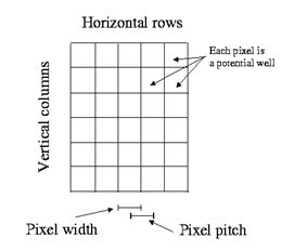
An actual CCD will consist of a large number of pixels (i.e., potential wells), arranged horizontally in rows and vertically in columns. The number of rows and columns defines the CCD size; typical sizes are 1024 pixels high by 1024 pixels wide. The resolution of the CCD is defined by the size of the pixels, also by their separation (the pixel pitch). In most CCDs the pixels are touching each other and so the CCD resolution will be defined by the pixel size, typically 10-20µm. Thus, a 1024×1024 sized CCD would have a physical area image size of about 10mm x 10mm.
A CCD chip is a metal oxide semiconductor (MOS) device. This means that its base, which is constructed of a material, which is a good conductor under certain conditions, is topped with a layer of a metal oxide. In the case of the CCD, usually silicon is used as the base material and silicon dioxide is used as the coating. The final, top layer is also made of silicon – polysilicon.
The basic unit of a CCD is the Metal Oxide Semi-conductor (MOS) capacitor
2.4. The basic unit of a CCD. (The MOS Capacitor)
Consists of:
Gate
A thin layer of metal or heavily doped polycrystalline attached to an electrode forms the gate. A bias voltage may be applied to the gate in order to change the shape of the underlying potential.
Oxide layer
A 0.1-micron thick oxide layer (usually SiO2) beneath the gate functions as the dielectric of the capacitor. The oxide is thickened to ~0.5 – 1.5 microns above the channel stops to insulate them from changes in the gate voltage.
Channel stop
The function of the channel stop regions is to confine charge. They are made of heavily doped p-type materials with an extra thickness of oxide over top. This makes them relatively insensitive to voltages applied to the gate and thus an effective potential barrier.
N-type buried channel
Most modern CCDs have buried channels. A buried channel is created by the addition of an n-type layer (~1 micron thick) between the gate and the oxide. An n-type (negative) semi-conductor is one, which has been doped with impurities of higher atomic number yielding an excess of free electrons in the conduction band. The effect of the n-type layer is to move the potential minimum back from the Si-SiO2 interface eliminating “fast surface states” which cause problems with charge transfer. The region where the signal charge collects, termed a channel, is within the n-type region.
P-type substrate
A p-type (positive) semi-conductor is one, which is doped with impurities of lower atomic number, resulting in “holes” in the valence states. The substrate is usually at least 15 microns thick.
Depletion region
In the depletion region, electrons from the n-type region have combined with holes from the p-type region. The result is the establishment of a potential difference because the n-type region becomes positively charged, while the p-type region becomes negatively charged. When photons are absorbed in the depletion region they form electron-hole pairs. The electrons are attracted to the n-type region. The holes diffuse away into the p-type region.
The silicon that forms the base and the top layer, however, is special in nature. It is a silicon material that is doped with, or made to contain, a small amount of some other material. Doping endows materials with special properties that can be exploited through different electrical means.
2.5.The physical point of view
To understand why doped silicon would have special properties and how those properties can be exploited, consider how silicon normally forms chemical bonds. Like carbon, a silicon atom can form up to four bonds with adjacent atoms. This is because silicon has four valence electrons that it can share to form bonds. In a crystal of pure silicon, all atoms (not on the surface of the crystal) would be perfectly bonded to four neighboring atoms; in this case, there are no extra electrons, but also no places where electrons are missing. You can see this by drawing the Lewis structures.
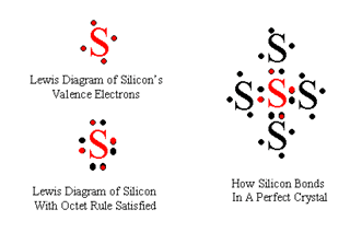
If, however, we introduce into the perfect crystal an element with only three electrons available for bonding, this atom will form three normal bonds and one bond with a “hole”, meaning that it is missing an electron. What is interesting here is that this “hole” actually can move around the entire crystal. An electron nearby can move to fill in the original hole, but in eliminating the original hole, it has created a new hole. Effectively, this hole is able to move around just a freely as a mobile electron. Such a material, one that contains extra holes, is called a p-type material.

A material with extra electrons is called an n-type material. In an n-type material, the “contaminating” element has five available electrons, so it makes the four usual bonds, but then has an extra electron left over. It is important to note that these materials are all neutral, and that extra electrons or extra holes in this case do not make the materials charged but merely come from what is left over or needed for a neutral atom to form four bonds.
Upon application of the right stimulus, the movement of the hole can be directed. This is one of the fundamental keys to the operation of the CCD. An electron is repelled by negative charge and is attracted by positive charge. A hole, however, is repelled by the positive charge and is attracted by negative charge. In this way, we can think of a hole as sort of a “positive” electron, even though it is not. As we can control the motion of electrons by applying different electrical fields or charges in the vicinity, so can we control the motion of holes?
If a p-type and an n-type material are brought into contact, a p-n junction is formed and a very interesting result occurs. Extra electrons from the n-type material will diffuse to the p-type material and fill in some of the extra holes from the p-type material. The diffusion and recombination of electron-hole pairs across the boundary directly results in the n-type material becoming positively charged and the p-type material becoming negatively charged. Recall that before the two materials were brought into contact and before diffusion occurred, they were both neutral. As diffusion occurs and the n-type and p-type materials become increasingly charged, an electric field is generated around the contact boundary. This electric field eventually slows and stops the diffusion of charge across the boundary. When diffusion stops, there are no more extra electrons or holes around the boundary; they have all recombined. This region surrounding the boundary in which electrons and holes have recombined is called the depletion region. Outside of the depletion region, extra electrons still remain in the n-type material and extra electrons remain in the p-type material. The depletion region is the key area, which can be used to create electrical devices. By applying a voltage to the depletion region, we can either increase or decrease the electric field across the depletion region. If the electric field is increased by an applied voltage (reverse bias), the depletion region is increased and less of any applied current can flow through the two materials. If the electric field is decreased by an applied voltage (forward bias), the depletion region is decreased and more applied current is allowed to flow through the two materials.
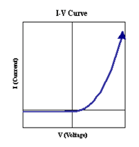
The importance of applying voltages to the depletion region (called biasing the p-n junction) is that it precisely allows us to control applied current through any p-n material. When the p-n junction is reversed-biased, an only infinitesimal amount of applied current can flow, which for all practical purposes is zero. This corresponds to the “off” state. When the p-n junction is forward-biased, current easy flows through the junction (because the smaller electric field does not impede the flow of charges as much). In fact, by plotting a graph of applied voltage versus current flow – an I-V Curve – we can see that the dependence of current flow on applied voltage across the junction is exponential. Forward bias corresponds to the “on” state. Thus, biasing of the junction through the application of voltages can be used to precisely control the motion of electrical charge.
3. Theory and Operation of CCD.
3.1.Introduction
A CCD in isolation is just a semiconductor chip. In order to turn it into a usable instrument it needs to be connected to some electronics to power it, control it and read it out. By using a few clocking circuits, an amplifier and a fast analogue-to-digital converter (ADC), usually of 16-bit accuracy, it is possible to estimate the amount of light that has fallen onto each pixel by examining the amount of charge it has stored up. Thus, the charge, which has accumulated in each pixel, is converted into a number. This number is in arbitrary `units’ of so-called `analogue data units’ (ADUs); that is, it is not yet calibrated into physical units. The ADC factor is the constant of proportionality to convert ADUs into the amount of charge (expressed as a number of electrons) stored in each pixel. This factor is needed during the data reduction and is usually included in the documentation for the instrument. The chip will usually be placed in an insulating flask and cooled (often with liquid nitrogen) to reduce the noise level. The whole instrument is often referred to as a CCD camera.
The electronics controlling the CCD chip are interfaced to a computer, which in turn controls them. Thus, the images observed by the CCD are transferred directly to computer memory, with no intermediate analogue stage, whence they can be plotted on an image display device or written to magnetic disk or tape.
3.2.CCD must perform 4 tasks to generate an image:
- 1) Generate Charge Photoelectric Effect
Silicon exhibits an energy gap of 1.14 eV. Incoming photons with energy greater than this can excite valence electrons into the conduction band thus creating electron-hole pairs. These pairs diffuse through the silicon lattice structure. The average lifetime for these carriers is 100 microsecs. After this time the e-h pair will recombine.
Photons with energy of 1.1 to 5 eV generate single e-h pairs. Photons with energy > 5 eV produce multiple pairs.
2) Collect Charge pixels: an array of electrodes (called gates)
3) Transfer Charge Apply a differential voltage across gates. Signal electrons move down vertical registers (columns) to horizontal register. Each line is serially read out by an on-chip amplifier.
4) Detect Charge individual charge packets are converted to an output voltage and then digitally encoded.
3.3How it works.
In a CCD, an array or matrix of electrodes controls the electrical field at different parts of the surface; these electrodes are called the gates. (CCD arrays can be either one-dimensional or two-dimensional, but here we will consider the one-dimensional array in detail, and then apply that information to understand the two-dimensional array.) This array of electrodes biases each small part of the surface differently, which allows any flow of charge on the CCD to be controlled.
The surface of the CCD is further broken down into smaller regions called pixels, or picture elements. This name is appropriate because they represent a single “grain” of the imaged object (just like you can see that your TV images appear to be made up of tiny “grains”). The array of electrodes applies a positive potential, (+Vg, a positive electric field) to two-thirds of each pixel, thus forward-biasing that portion of the pixel. Let’s represent the first third of the pixel by (1, the second third by (2, and the last third by (3. So, (1 and (3 are at a positive potential of +Vg, and (2 is at a lower potential, Vs.
When light or photons of high enough energy strike the surface, electrons are usually liberated from the surface. For every electron liberated, a hole is created simply by the act of the electron leaving. Thus, incident photons create electron-hole pairs. The hole, being effectively positive, is repelled by the applied positive potential into the base of the chip. The electron, however, is captured in the nearest potential well. The more light incident on a pixel, the more electrons captured in the potential wells. Thus, differences in the intensity of incoming light are “recorded” by the number of electrons collected in each potential well.
So now the challenge is to extract information from these “electron-collecting bins” (which may also be thought of as tiny capacitors). To do this, the charge packets (the collection of electrons in each well) must be transferred to another device for data processing. This is accomplished by sequentially changing the applied voltage at the three parts of each pixel or we may call it clocking out the CCD (The 2nd step).
A two-dimensional CCD is composed of channels, or rows along which charge is transferred. Each channel is essentially a one-dimensional CCD array. Charge is prevented from moving sideways by channel stops, which are the narrow barriers between the closely spaced channels of the CCD.
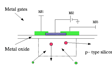
3.4.How it is clocked out.
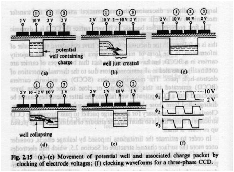
The figure below shows a cross section through a row of a CCD. Each pixel actually consists of three electrodes IØ1, IØ2, and IØ3. Only one of these electrodes is required to create the potential well, but other electrodes are required to transfer the charge out of the CCD. The upper section of the figure (section 1) shows charge being collected under one of the electrodes. To transfer the charge out of the CCD, a new potential well can be created by holding IØ3 high, the charge is now shared between IØ2 and IØ3 (section 2). If IØ2 is now taken low, the charge will be fully transferred under electrode IØ3 (section 3). To continue clocking out the CCD, taking IØ1 high and then taking IØ3 low will ensure that the charge cloud now drifts across under the IØ1 electrodes. As this process is continued, the charge cloud will progress either down the column, or across the row, depending upon the orientation of the electrodes.
The figure below (called a clocking diagram) shows the progression under which each electrode is held high and low to ensure that charge is transferred through the CCD.
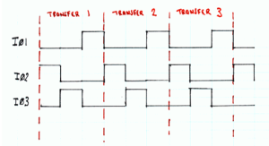
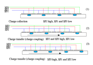
Initially, IØ2 is high – usually to around 12V, and the charge is held under that electrode as in (1) previously. When IØ3 is held high, and IØ2 is taken low (usually 0 V), the charge migrates under the IØ3 electrode (as in (2)). Finally, taking IØ1 high and IØ3 low transfers the charge under IØ1 (as in (3)). This process is repeated in transfer 2 and transfer 3, the charge has now been moved three pixels along. This process is known as charge coupling (hence CCD).
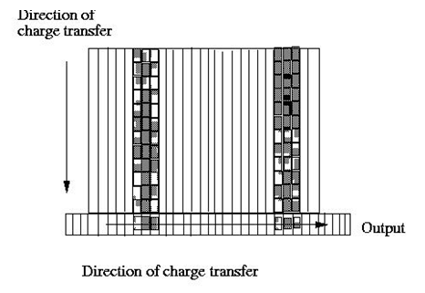
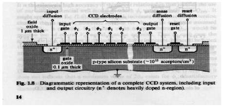
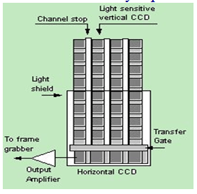
For most of the CCD, the electrodes in each pixel are arranged so that the charge is transferred downwards along the columns. Hence, during the CCD clocking operation, rows are transferred downwards to the final row (the readout register), which is used to transfer the charge in each pixel out of the CCD so it can be measured.
In the read out register, the electrodes are arranged so that the charge is transferred in the horizontal direction, along the readout register.
3.5.How its charge is measured and Read out.
The final process on the CCD is the reading of each pixel so that the size of the associated charge cloud can be measured. At the end of the readout register is an amplifier which measure the value of each charge cloud and converts it into a voltage, a typical conversion factor being around 5-10µV per electron with “typical” full well values being about 100,000 electrons or so.
A CCD camera will consist of the CCD chip, and associated electronics, which is used at this point to amplify the small voltage on the CCD, remove noise components, digitize the pixel values and output the values of each pixel for example, to a PC, where the image can be processed in software and the image displayed. The CCD is an analogue device, and the analogue voltage values are converted into a digital form by the camera electronics.
Calculating the length of time required to read out any particular image is straightforward. Before doing so however, it is necessary to understand how the CCD is read out. As shown in figure, the CCD will be read out by clocking each row down the CCD until it reaches the serial (readout) register. Once in the register, pixels are shifted across, one at a time, into the readout amplifier.
We will have two CCDs, one detecting the long wavelengths and one detecting the short wavelengths. To improve readout time and to provide some redundancy, each CCD has two read out ports, one at the bottom right of the CCD and one at the bottom left.
Charge is transferred along the parallel register (parallel to the channel stops), that is by “clocking the gates, each row is moved in unison to the serial register where the pixels are moved one by one to the amplifier.
4. How CCD record color or distinguish among photons of different energies (Color Differentiation)
In imagers or CCD cameras, CCDs are only part of the whole device. A lens is required to properly focus the incident radiation from the object onto the array. In addition, since the pixels themselves are monochrome, there must be a way to select for the wavelengths of light incident on the array. Colored filters are thus used to record colors in the case of visible light. In most digital cameras, a color filter array registers the intensity of a single color at each pixel. By interpolation, algorithms use the color intensities at nearby pixels to estimate the intensity of a color at each pixel. This is how a full-color image is generated. A single picture made by a CCD imager that is only 500 pixels by 500 pixels holds the same amount of raw information as a 100,000 word book! In addition, the number of electrons collected is proportional to the energy of the incident photons. So mathematically, the energies of the photons liberated can be calculated.
5. Some aspects of CCD behavior (Characteristics)
5.1. Charge Transfer Efficiency (CTE).
Charge in a typical pixel is transferred several hundred thousand times before being read out. Thus the Charge Transfer Efficiency (CTE) is very important.
CTE is the percent of charge transferred from 1 pixel to the next. This number needs to be very close to 100 %. Here’s why:
- • Consider the middle pixel of a 1024 x 1024 CCD. Charge stored in this pixel will be moved 1024 times (512 transfers along the parallel register, 512 along the serial register.)
- • Let’s say the CTE is 98 %
- • By the time it is read out it has (0.981024) x 100 % = 0.0000001 % of its original charge. This is not good.
- • A good CTE today is 99.999 %. With this CTE the center pixel will have 99 % of its original charge by the time it is read out.
5.2. Quantum Efficiency (QE) or Linearity.
On the whole, the eye is not a linear detector (except over very small variations in intensity) and has a logarithmic response. An important consideration in a detector is its ability to respond linearly to any image it views. By this we mean that if it detects 100 photons it will convert these to 100 electrons (if we had 100% QE) and if it detects 10000 photons, it will convert these to 10000 electrons. In such a situation, we say that the detector has a linear response. Such a response is obviously very useful as there is no need for any additional processing on the image to determine the ‘true’ intensity of different objects in an image.
Not every photon falling onto a detector will actually be detected and converted into an electrical impulse. The percentage of photons that are actually detected is known as the Quantum Efficiency (QE). For example, the human eye only has a QE of about 20%, photographic film has a QE of around 10%, and the best CCDs can achieve a QE of over 80%. Quantum efficiency will vary with wavelength.
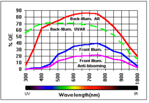
The quantum efficiency (Q.E.) of a sensor describes its response to different wavelengths of light (see chart). Standard front-illuminated sensors, for example, are more sensitive to green, red, and infrared wavelengths (in the 500 to 800 nm range) than they are to blue wavelengths (400 – 500 nm). This is most noticeable in tri-color imaging with color filters, where exposures taken with the blue filter need to be much longer than the exposures taken with the green and red filters, in order to achieve proper color balance.
Back-illuminated CCDs have exceptional quantum efficiency compared to front-illuminated CCDs. This is due to the way they are constructed. How do you make a back-illuminated CCD? Simply, Just take a front-illuminated CCD, thin it to only 15µm thick and mount it upside down on a rigid substrate. The incoming light now has a clear shot at the pixel wells without those pesky gate structures blocking the view.
Typical Q.E. curves for front- and back-illuminated CCDs are shown in the previous page.
Note that CCDs with anti-blooming have about 1/2 the Q.E. of those without anti-blooming. CCDs with backside illumination can boost quantum efficiency to over 85%.
5.2.1.Frontside vs. Backside Illumination.
- • Frontside Illumination:
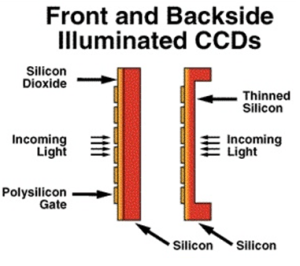
Limited by absorption of blue photons by relatively thick (5000 A) poly-silicate gates. Absorption depth for 4000 A photon is only 2000 A. Also, surface reflectivity increases with decreasing wavelength. Hence thick frontside illuminated devices have good QE only in the red.
• One way of improving QE is by “back-side illuminating”.
Traditionally, CCDs were illuminated on the front side, meaning the side with the gates. Many of the blue photons were absorbed by the relatively thick (0.5 micron) gates. At longer wavelengths interference effects reduce the QE. Today it is possible to make backside-illuminated devices. In these devices the silicon substrate is thinned to ~15 microns and the gate side is mounted against a rigid surface. An enhancement layer is also added which creates an electric field that forces electrons toward the potential wells. Backside illuminated devices have higher QE especially in the blue and UV portion of the spectrum. QE may also be enhanced by the addition of an anti-reflective coating.
• Backside Illumination:
- o For high and stable QE the backside of the CCD must be negatively charged to drive signal electrons towards the front surface. Three backside treatments:
- a) UV flooding creates lots of free electrons. Some of these electrons have enough energy to escape to the back surface thus creating a small surface voltage, which in turn attracts and accumulates a thin layer of holes; hole gradient sets up an intense electric field in the silicon (100,000 V/cm). But, doesn’t last unless the detector stays at -95 C (or lower).
- b) Flash Gates deposit mono-atomic layer of gold or platinum; causes silicon electrons to tunnel through the native oxide layer and generate a surface potential equal to the work function difference between the metal and the silicon. Unfortunately, in a vacuum positive charge is observe to buildup in the native oxide layer. So invent, biased flash gate – now you have a shutter and control of the QE! Positive bias, charge is swept towards the backside – no QE; negative bias, charge is swept to the frontside lots of QE
- c) Boron doping ion implants provide a permanent hole layer (i.e. thin layer of hole accumulation). Manufacturing process requires heating of the device to anneal the damage down during the implantation process. This is best accomplished using a scanning high energy pulsed laser directly on the immediate backside surface
- • Phosphor Coatings:
- o Converts incoming UV photons to longer wavelength photons.
- o Can evaporate under conditions of high vacuum.
- o Scattering of light from Target pixel to adjacent pixels in the UV –> mostly a problem for front illuminated devices as on the backside the phosphor is in direct contact with the silicon separated only by the thin native oxide layer
- o multiple e-h pair generation is not possible; Phosphor only emits one visible photon per incoming photon
5.2.2.Blooming vs. Anti-Blooming.
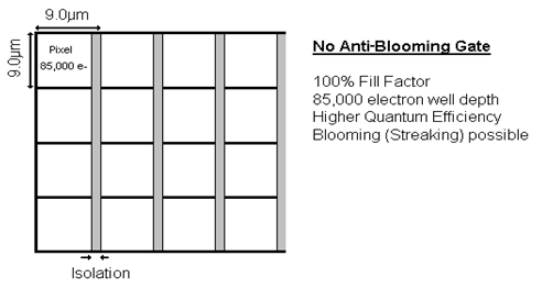
Some sensors offer an optional anti-blooming gate designed to bleed off overflow from a saturated pixel. Without this feature, a bright star which has saturated the pixels (much greater than 85,000 electrons) will cause a vertical streak. This can be irritating at best, and if the streak bleeds onto your target object, there is no way to recover the lost data.
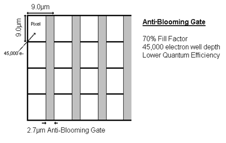
Anti-blooming gates built into the CCD occupy about 30% of the pixel area. The result is a 70% fill factor and reduced sensitivity and well depth. The reduced sensitivity means that you have to expose almost twice as long to get the same signal level as a CCD without the anti-blooming feature. Also, the area of the CCD occupied by the anti-blooming gate leaves a significant gap between pixels, reducing the effective resolution of the sensor.
Because of these drawbacks, users of CCDs without anti-blooming gates have chosen an alternate method to avoid blooming. Rather than taking a single long exposure in which blooming is almost certain to occur, take several short exposures, in which the brightest objects haven’t begun to bloom, and stack the exposures together with image processing software. The signal-to-noise ratio remains the same as in the longer exposure, but the result is free of blooming.
Since opinions vary on which is the ideal method to achieve anti-blooming, we offer the following guidelines for selection:
1) If non-blooming of bright objects is critical for your application, and if guiding twice as long to overcome the loss in sensitivity is not bothersome, then the anti-blooming option may be for you.
2) For tri-color imaging, front-illuminated CCDs already have low response in the blue. Therefore, the lessened response with the anti-blooming gates will require extremely long exposures with the blue filter to obtain good color balance. For this and other applications that require good response to blue light, you may wish to use the stacking method to avoid blooming.
5.3.Wavelength range.
CCDs can have a wide wavelength range ranging from about 400nm (blue) to about 1050nm (Infra-red) with peak sensitivity at around 700nm. However, using a process known as back thinning, it is possible to extend the wavelength range of a CCD down into shorter wavelengths such as the Extreme Ultraviolet and X-ray.
5.4.Dynamic Range.
The ability to view bright and faint sources correctly in the same image is a very useful property of a detector. The difference between a brightest possible source and the faintest possible source that the detector can accurately see in the same image is known as the dynamic range. When light falls onto a CCD the photons are converted into electrons. Consequently, the dynamic range of a CCD is usually discussed in terms of the minimum and maximum number of electrons that can be imaged. As more light falls onto the CCD, more and more electrons are collected in a potential well, and eventually no more electrons can be accommodated within the potential well and the pixel is said to be saturated. For a typical scientific CCD this may occur at around 150,000 electrons or so. The minimum signal that can be detected is not necessarily one electron (corresponding to one photon at visible wavelengths). In fact, there is a minimum amount of electronic noise, which is associated with the physical structure of the CCD and is usually around 2-4 electrons for each pixel. Thus, the minimum signal that can be detected is determined by this readout noise.
In the example above, the CCD would have a dynamic range of 150,000:4 (taking the upper noise level). But this dynamic range is also dependent on the ability of the electronics to be able to fully digitize all of this dynamic range.
5.5.CCD Camera Characteristics.
There are many important characteristics that should be taken into account when buying a camera. Even when a camera should excel in all categories, the buyers sometimes have to make a compromise. The reason for this is that sometimes some of these features are more expensive to include than other. The following will inform about some of the most important features of a CCD camera.
5.5.1.Sensitivity.
This analyzes the variation between different levels of brightness. A higher sensitivity could be able to detect the minute differences between different levels of brightness.
5.5.2.Transfer Function.
Transfer Functions analyze the ratio of output modulation to input modulation. This is a mathematical expression that tells you how accurate is the link between the camera output and the light intensity.
5.5.3.Resolution.
The resolution is determined by the number of sensor elements on the CCD chip. A higher number of elements will increase the detail observed from a particular image. On a CCD camera the resolution is usually defined in the number of pixels for the x and y dimension of the camera. A high resolution will be extremely important when trying to observe the fine details of an image. In order to have high resolution a CCD camera must have:
- • At least an array of 1 mega pixels. Such as a 1000 by 10000 pixel camera. And must have few bad pixels. Which are pixels that are dead or not responding appropriately.
- • A cooling system to reduce thermal noise.
- • A high readout clock frequency.
Black and White cameras have an extra edge over Color cameras. Since the resolution for color cameras is reduce by 1/3 compared to a B&W camera of the same pixel count. This is due to the fact that color cameras usually use 3 types of sensor to detect color images, one for Red, one for Blue and another for Green.
5.5.4.Low light levels Capture.
A camera that has to work with low light level captures must have a low signal to noise ratio. The least level of light that can be detected must be higher than the noise level in the system. This sometimes fudges the low level signals against the background noise. There are many sources for this noise, such as:
- • Fixed Pattern Noise (FPN) which is caused by defects in the sensor array. This noise pattern is usually constant on all expositions. This source is usually inversely proportional to the quality of the sensor array. However higher quality implies a more costly array.
- • Thermal noise, which can be reduced by cooling the sensor below 30
- • Any uncooled electronic will emit charges which are collected and added to the noise level.
- • Electronic noise, which is produced by the rapid movement of charges during the readout process. It can be lowered by choosing moderate clock frequencies for the charge transfer to the readout section of the system.
- • Reset noise, which is produced when not every charge is drained out of the CCD elements. This charge leftover will influence the value for the next readout on this CCD element.
5.5.5.Capture speed.
This is important in any field of optical research since you always want to have a fast snapshot of viewed system during any event. Since all events in physics change rapidly with time, a fast camera will reduce the blurriness of the data observed a system drifting out across time.
The speed of a digital camera depends on several factors:
- • The sensor architecture, a full frame digital camera is slower than a frame transfer camera or a interline transfer due to the higher density of the sensor on the chip.
- • Number of pixels: the digital camera, at the same clock frequency, is fast if it has few pixels.
- • Clock frequency, a higher clock frequency makes a fast charge transfer possible. However, increasing the clock frequency higher than 25 MHz increases the signal to noise ratio.
5.5.6.Spectral response.
This informs us of how efficiently the camera picks up photons of different wavelength. In laser research this characteristic of the CCD sensor is highly important since lasers are usually tuned to a very specific frequency. Usually the detection range of the sensor array is around the visible range, passing through the infrared and up to 1000 nm. However, any wavelength other than those, the detection is difficult.
Spectral sensitivity is also referred as Quantum Efficiency (Q.E.) as described before. A perfect CCD sensor has a Q.E of 1. This means that for every photon falling upon the sensor, an electron or charge is produce. In reality, the Q.E. of most cameras max. out at 0.7. That is, for every 10 photons, 7 electrons are produce by the CCD.
5.6.Pixel size and Field of view.
In images observed close to the optical axis an angular displacement is simply proportional to a linear displacement in position in the focal plane. The constant of proportionality is usually called the plate scale (a name which betrays its origin in photographic techniques) and is traditionally quoted in units of seconds of arc / mm. That is: p=∆”/∆ (1)
Where p is the plate scale in seconds of arc / mm, ∆ is a displacement and ∆mm is the corresponding displacement in the focal plane in mm. If you know the plate scale and the size of either a single pixel in the grid or the linear size of the CCD then it is trivial to use Equation (1) to work out either the angle subtended by a single pixel or the field of view of the CCD respectively. The manual for the instrument that you are using will usually quote a value for the plate scale. However, if necessary it can be calculated from other parameters. By simple geometry the plate scale is the reciprocal of the effective focal length of the system:
p/ =1/ f (2)
where f is the effective focal length of the system and p/ is the plate scale in units of `radians / whatever units f is in’. Thus, for f in meters and applying the factor for converting radians to seconds of arc:
p = 206.26 / f (3)
f is itself related to the diameter of the primary mirror, D, and the focal ratio, F:
f = F. D (4)
At larger distances from the optical axis there is no longer a simple linear relation between angular displacement on the sky and displacement in position in the focal surface. That is, p varies as a function of position in the focal surface. This effect is usually not important in instruments containing a single chip because of the small size of individual CCDs. However it may be important if a grid of chips is used.
6. Different types of CCDs.
There are three different types of architecture employed in the manufacturing of CCD cameras. The main difference from all these designs is in how they received and process the information. These designs are:
- • Full-Frame CCD
- Interline Transfer CCD
- • Frame-Transfer CCD
6.1.The Full-Frame CCD
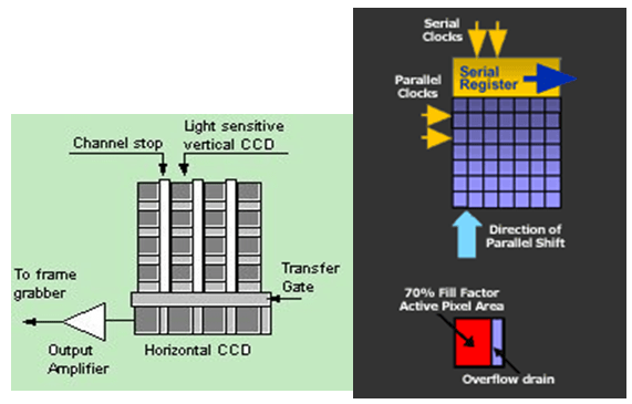
After the exposure the Full-Frame CCD must be covered from light during the readout process. The charge from the bottom row of the potential wells is ‘shifted’ to one side in order to be read one by one. When the whole row is read, the next row drops down and the whole process begins again. Once this has been done, the device is ready to receive the input from another picture.
6.2.The Inter-line-Transfer CCD
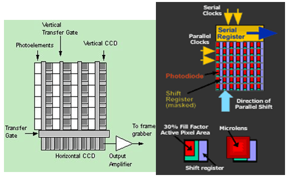
Every second column within an Inter-line-Transfer CCD is covered by an opaque mask. These covered areas contain the wells that are used in the readout process. After the exposure, the charged packets in each exposed cell is shifted into the adjacent opaque masked wells. From here, the charge is being ‘shifted’ as in the Full-Frame CCD. The advantage of this is that while the charge is being ‘shifted’ the exposed wells can accumulate in the next image. But, the disadvantage is that only 50% of the surface is exposed. This method is fairly rapid.
6.3.Frame Transfer CCD
The frame transfer CCD imager has a parallel register divided into two distinct areas. The upper area is the image array, where images are focused and integrated. The other area, the storage array, is identical in size and is covered with an opaque mask to provide temporary storage for collected charge. After the image array is exposed to light, the entire image is rapidly shifted to the storage array. While the masked storage array is read, the image array integrates charge for the next image. A frame transfer CCD imager can operate continuously without a shutter at a high rate. The front illuminated Frame Transfer CCDs suffer the same fate as the Full Frame CCDs, that is a reduced QE in the visible with a particularly low QE in the blue. The combination of back illuminated (CCD EEV 57), the shutterless operation, relatively high frame rates and very high QE is very desirable to have in a camera system.
7. Noise sources in CCD.
7.1.Introduction
When a CCD image is taken, noise will appear as well as the main CCD image. Noise can be thought of as unwanted signal, which doesn’t improve the quality of the image. In fact, it will degrade it. The main problem with noise is that most noise is essentially random, and so cannot be completely removed from the image. For example, if we know that a noise source contributes 10 units on each image we can subtract those 10 units from the image. If we only know that the noise is ‘around’ 10 units, then we can’t completely remove all of this noise (as we don’t know its exact value).
Noise manifests itself during two main processes: the collection of electrons and the transfer of charge packets. During the collection of electrons, noise stems from thermal processes, light pollution, and the generation of electron-hole pairs in the depletion regions. During charge-transfer, noise stems from transfer inefficiency.
7.2.The main contributions to CCD noise
7.2.1Noise on the image itself (“shot noise”)
The detection of photons by the CCD is a statistical process. If images are taken over several (equal) time periods, then the intensity (the number of photons recorded) will not be the same for each image but will vary slightly. If enough images are taken, it will be seen that the deviation in intensity found for each image follows the well-known Poisson distribution. In effect, we cannot be sure that the intensity we have measured in a particular image represents the “true” intensity, as we know that this value will deviate from the average. It is this deviation, which is considered to be the noise associated with the image. As the deviation is known to follow a Poisson distribution, we know that the likely deviation will be plus or minus the square root of the signal intensity measured. Thus, if we measure a signal intensity of one hundred photons, then the noise on this signal will be ten photons. If we measure a signal intensity of one thousand photons in the image, then the noise on this signal will be about thirty-one photons.
7.2.2.Thermally generated noise
Additional electrons will be generated within the CCD not by the absorption of photons (i.e. the signal) but by physical processes within the CCD itself. The number of electrons generated will be dependent on the operating temperature of the CCD and hence this noise is known as thermal noise (sometimes also known as dark noise). As with the detection of the signal, the same number of electrons will not be generated in equivalent periods of time, as the thermal noise will also have a Poisson distribution.
7.3.Some of the Physics behind the generation of various types of noise within a CCD
7.3.1.Dark current
Even in the absence of light, thermally generated electrons will be collected in the CCD and will contribute to the overall signal measured. There are three main contributions to dark current:
- • Thermal generation at surface states.
- • Thermal generation within the bulk silicon.
- • Thermal generation in the depletion region.
The vast majority of the thermally generated electrons are generated at the surface states. Interface states can exist in the forbidden energy gap between the valence and conduction bands (such states do not exist in a perfect lattice and are caused by the change in energy within the lattice due to the introduction of an impurity atom or lattice defect). An electron can be excited by absorption of a photon with insufficient energy to excite the electron into the conduction band but with sufficient energy to excite it into the mid-band interface state. A second photon can then excite the electron into the conduction band.
However, if the interface states are filled up by free carriers then the dark current will be drastically reduced. Such a process can be achieved by operating the CCD in inversion which is a technique used by all modern CCDs. When the CCD is operated in inverted mode, holes from the channel stops migrate to fill the interface states. Two of the three electrodes defining a pixel are driven into inversion to drastically reduce the dark current (it is not possible to invert all three electrodes as a potential well is still required to collect charge). If a CCD is not inverted, then the dark current generation rate may be as high as several hundreds of thousands of electrons per pixel per second (at room temperature) whereas an inverted CCD will have a much lower generation rate of about ten thousand electrons per pixel per second.
If such a CCD is read out a number of times per second (for example in a video camera) then the dark current at room temperature is low enough not to significantly interfere with image quality. However, if the CCD is only read out once a second (or less frequently) then the number of thermally generated electrons will be too high for adequate image quality. Hence, additional measures need to be taken.
The simplest way to reduce the dark current is to cool the CCD as dark current generation is temperature related.
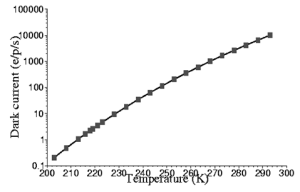
The figure above shows the variation in dark current with temperature for a CCD with a room temperature dark current of 10,000 electrons/pixel/s. There are a number of ways in which a CCD can be cooled, the easiest is to use liquid Nitrogen but thermoelectric coolers (Peltier coolers) can be used, and in space the CCD can be cooled with a direct connection to a passive radiator.
A second way of reducing the dark noise in a CCD is to use a Multi-Pinned Phase (MPP) device. In an MPP device, it is possible to operate the CCD with all three electrodes phases driven into inversion. This is accomplished by adding a suitable dopant under one of the phases during CCD fabrication. The presence of the additional dopant under one of the phases alters the potential under that phase so that there is still a potential well present during integration when all the electrode phases are at clock low level (usually zero volts). Dark current is now only generated in the bulk silicon reducing the dark current to about 300 electrons/pixel/signal.
7.3.2.Readout noise
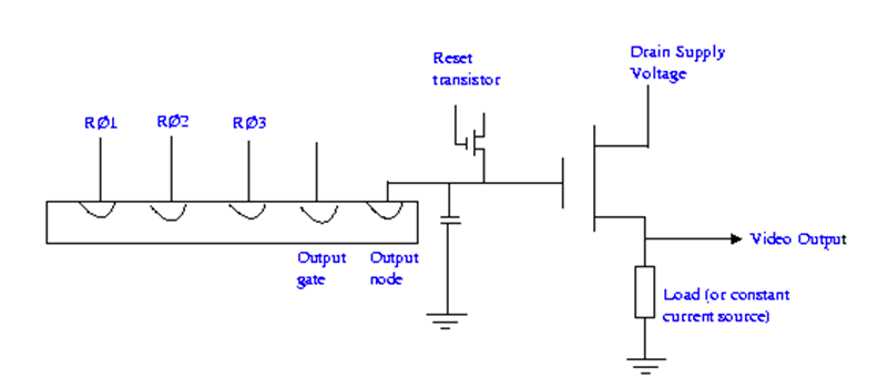
The ultimate noise limit of the CCD is determined by the readout noise. The readout noise is the noise of the on-chip amplifier which converts the charge (i.e. the electrons) into a change in analogue voltage using:
Q= CV where Q is the charge on the output node, and C is the output node capacitance. V is the voltage sensed by the on-chip amplifier operating as a source follower.
The figure above shows a schematic of a typical CCD output section. The charge in a pixel is transferred onto the output node where the change in voltage caused by this charge is sensed by the on-chip amplifier.
The on-chip amplifier will have an associated noise performance, which is typically 1/f at low sampling frequencies with a white noise floor at higher sampling frequencies. The sampling frequency corresponds to the rate at which each pixel is read by the CCD.
The figure to the right shows the readout noise response versus the sampling frequency for a typical CCD. It can be seen that as the sampling frequency increases, the root mean square value of the read out noise increases.
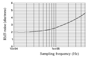
A large amount of effort has been dedicated to reducing the CCD readout noise, as this noise value will ultimately determine the dynamic range and should be as low as possible, particularly when detecting very faint sources for example, detecting photons at X ray energies such as in the XMM-Newton mission. Noise values of 2-3 electrons rms (root mean square) are now typical for many CCDs but some companies have recently claimed a noise resolution of less than 1 electron rms.
7.3.3. Power
CCDs themselves consume very little power. During integration, only a very small current is flowing and the CCD consumes only 50mW or so. Whilst the CCD is being clocked out more power can be consumed but this is typically only several Watts or so. Of course, the electronics required to operate the CCD and process images can consume much more power.
7.3.4.Non-linearity
As mentioned before, CCD chips have a wide dynamic range within which their response is essentially linear. However, if the illuminating light is sufficiently bright the response will become non-linear and will ultimately saturate (that is, an increase in the intensity of the illumination produces no change in the recorded signal). In principle the response in the non-linear region can be calibrated. However, in practice, the onset of saturation is sufficiently rapid that it is more sensible to limit exposures to the linear region. In order to prevent saturation it is usual to a take a series of short exposures rather than a single long exposure of equivalent duration. The individual short exposures can then simply be added during the data reduction.
7.3.5.Pixel sensitivity; flat fielding
Due to imperfections in the manufacturing process the sensitivity of the pixels will vary slightly (usually by a few percent) across the grid. This effect is essentially random, and is not a function of, for example, position on the grid. The relative sensitivities of the pixels can be calibrated by imaging an evenly illuminated source, such as the twilight sky, and examining the variation in values recorded. Once this calibration is known, images can be corrected to the values they would have had if all the pixels had been uniformly sensitive. This correction is known as flat fielding and images of evenly illuminated sources are known as flat fields. The pixel-to-pixel sensitivity variations change with wavelength, so the flat fields should always be acquired using the same filter as the observations of the target objects.
8. Some methods to test the performance of CCD camera.
There are many ways to test the performance of a CCD camera. All depends of the criteria that we use to judge the camera. In laser research, the most important characteristic of the camera is the linearity of the incident light versus the charged recorded by the device. The simplest of the methods would be to just take a picture with camera covers on. This in theory should produce a totally black image, devoid of any features or objects. However, most CCD cameras will produce a dark background with small white spots on it. These are by-products of thermal noise. Also, the CCD doesn’t record the total range of intensities. The recording is made in discrete zones. With the intensity value of small surface elements being the same. The result of this is that every small element gives an average value of the light intensity over that given surface. This leads to another test of the accuracy of the CCD sensor. A surface composed of a series of dark and bright fringes could be composed. The camera used to record the image can only show a finite amount of detail of the lines. If the number of lines is bigger than the number of pixels along an axis, a process called aliasing occurs. Where the frequency of the lines appear to be less than they are since a section of the fringes had to be sampled as the same value. The maximum frequency of such changes between intensity that can be recorded by a camera is called Nyquist frequency. On the other hand, there are mathematical analyses that can help us find the quality of the date gathered by our CCD array. One of this methods is the Modulation Transfer Function (MTF) which measures the ratio of output modulation versus input modulation and other is the Point Spread Function (PSF), which measured the how blurred is the image taken compared with the real object.
9. Why CCD is so great. (Advantages and Early limitations)
The answer to the above question lies in its resolution. CCDs provide extraordinary detail for objects either very far away or very small in size – resolution that was hitherto impossible to attain. This resolution is a result of the large number of pixels in the CCD array – the more pixels, the finer the detail that can be achieved. Typically, modern CCDs comprise anywhere from about one thousand to about half a million pixels.
The principal advantages of CCDs are their sensitivity, dynamic range and linearity. CCDs are sensitive to a broad range of wavelengths and are much more sensitive to red light than either photographic plates or the photomultiplier tubes used in photoelectric. However, they have a poor response to blue and ultra-violet light. A typical dynamic range is about 105, corresponding to a range of about 14.5 magnitudes.
Thus, CCDs are nearly ideal detectors because of the following properties:
- • High Quantum Efficiency (QE) compared to photographic film.
- • Large dynamic range.
- • High linearity.
- • Fairly Uniform response.
- • Relatively Low noise.
- • It is Digital!
Early Limitations:
- • Low coverage area.
- • Poor blue response.
- • Read Out Noise Dominated for Spectroscopy.
- • Low light level deferred Charge Transfer Problems.
10. Some biomedical applications of CCD.
This small, electrical device is familiar to astronomers, physicists and engineers but now even some biologists and chemists are beginning use CCDs in their research. You have likely encountered it before, as CCDs are used in facsimile machines, photocopiers, bar-code readers, closed-circuit television cameras, video cameras, regular photographic cameras, or other sorts of sensitive light detectors. In fact, CCDs have a wide range of applications – everything from reconnaissance and aerial mapping to medicine, micro technology and astronomy.
CCDs are used in a variety of different imaging devices. Linear imaging devices (LIDs) employing CCDs are typically used in facsimile machines, photocopiers, mail sorters, and bar code readers, in addition to being used for aerial mapping and reconnaissance. Area imaging devices (AIDs) employing CCDs are used for closed-circuit television cameras, video cameras, and vision systems for robotics and as film for astronomical observations. CCDs are also used in drug discovery in combination with DNA arrays in a process called Multi-Array Plate Screening (MAPS).
CCD cameras have revolutionized the way of taking and recording images. They have extended the range of faint objects doctors can study. One of the other huge advantages to using CCD cameras is the ability to convert the gathered analogue information into digital information, which can be analyzed using computer software.
10.1.Multi-Array Plate Screening (MAPS)
In MAPS, potential drugs are applied to their targets in a microtiter plates. Their degree of binding to the target – and thus their potential ability as effective drugs – is assessed by the amount of light emitted from the well through either laser-induced fluorescence, radioactive scintillation, or chemiluminescence. The CCD must be cooled to cryogenic temperatures of about -100°C to minimize noise from thermal photons. CCD cameras are able to detect both RNA and DNA in amounts as low as 30,000 molecules, which are about 5.0 x 10⁻²⁰ moles. The benefit of using CCD cameras in MAPS is that no amplification of the nucleotides is required, which reduces cost and error and saves time.
10.2.X-ray Detection using a CCD
A CCD is a detector that can be used as an energy-dispersive detector that will give the energy of an x ray and the location where an x ray hit. Each pixel on the CCD can be used as an individual energy-dispersive detector because in the soft x-ray range the generation of electron-hole pairs is dominated by the direct band gap. The direct band gap in silicon has an energy gap of 3.65 eV. In the x-ray range the number of electron-hole pairs created in silicon when an x ray is absorbed is proportional to the energy of the x ray. In order to use each pixel as an energy dispersive detector, the pixels on the CCD must work in single-event count mode.
In order to acquire the energy information from an X ray, only one X ray must be captured in a pixel. If more than one x ray is deposited in a pixel, the pixel will contain the energy information from both of the events and there is no way to separate the energy. As long as one x-ray event is captured in one pixel, then the CCD can be used as an energy dispersive detector.
10.3.What Are the Non-Imaging Applications of the CCD?
Non-imaging applications of CCDs include signal processing, memory applications, video integration, transversal filtering, and MTI filtering for radar. Again, non-imaging applications fall under the categories of either signal processing or delay line applications.
11. Future of CCD.
The future of imaging devices, however, is not likely to be the CCD. The CMOS or Complementary Metal Oxide Semiconductor image sensor appears to be the future of imaging, because it is fabricated using essentially the same CMOS process as the large majority of modern integrated circuits, which include microprocessors and dynamic random-access memories (RAMs). CCDs, on the other hand, are fabricated using a variant of practically obsolete N-MOS fabrication technology, which is basically only used now in the fabrication of CCDs. What has kept CMOS image devices from replacing CCDs is the trade-off in image quality; there is more noise in CMOS devices, and unwanted signals from various sources degrade the input signal. For many applications requiring that every photon count, the CMOS is simply not sensitive enough. For the meantime, CCDs will be used in imaging devices where resolution is very important, and CMOS imaging devices will be used when their cheaper cost outweighs the benefit of higher resolution.

السلام عليكم اخي .. عندي استفسار
حاجز الجهد الموجود بين البوابات (مسجلات الازاحة ) هل هو مثل جهد الايقاف فى التجربة الكهروضوئية
ام مثل منطقة النضوب فى الوصلة الثنائية PN Junction
LikeLike